The most remarkable characteristic of MOS tubes is their good switching characteristics, so they are widely used in circuits that require electronic switches. Commonly used are switching power supplies and motor drives, as well as lighting dimming.
There are several special requirements for the current MOS driver.
1, low-voltage applications When using 5V power supply, this time if the traditional totem pole structure is used, because the transistor of the triode has a voltage drop of about 0.7V, the voltage actually added to the gate is only 4.3V. At this time, we have a certain risk in choosing a MOS tube with a nominal gate voltage of 4.5V. The same problem occurs when using 3V or other low voltage power supplies.
2. Wide voltage application input voltage is not a fixed value, it will change with time or other factors. This change causes the driving voltage supplied to the MOS transistor by the PWM circuit to be unstable.
In order to make the MOS tube safe under high gate voltage, many MOS tubes have a built-in voltage regulator to forcibly limit the amplitude of the gate voltage. In this case, when the supplied driving voltage exceeds the voltage of the Zener diode, a large static power consumption is caused.
At the same time, if the voltage of the resistor is used to reduce the gate voltage, the MOS transistor works well when the input voltage is relatively high, and the gate voltage is insufficient when the input voltage is lowered, causing the conduction to be insufficient, thus increasing the power consumption. .
3, dual voltage application
In some control circuits, the logic uses a typical 5V or 3.3V digital voltage, while the power section uses a voltage of 12V or higher. The two voltages are connected in a common manner.
This raises a requirement that a circuit is required to enable the low-voltage side to effectively control the MOS transistor on the high-voltage side, while the MOS transistor on the high-voltage side also faces the problems mentioned in 1 and 2.
In these three cases, the totem pole structure can not meet the output requirements, and many off-the-shelf MOS driver ICs do not seem to contain the structure of the gate voltage limit.
So I designed a relatively versatile circuit to meet these three needs.
The circuit diagram is as follows:
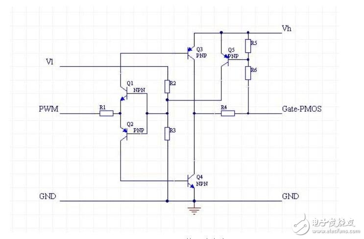
Figure 1 Drive circuit for NMOS 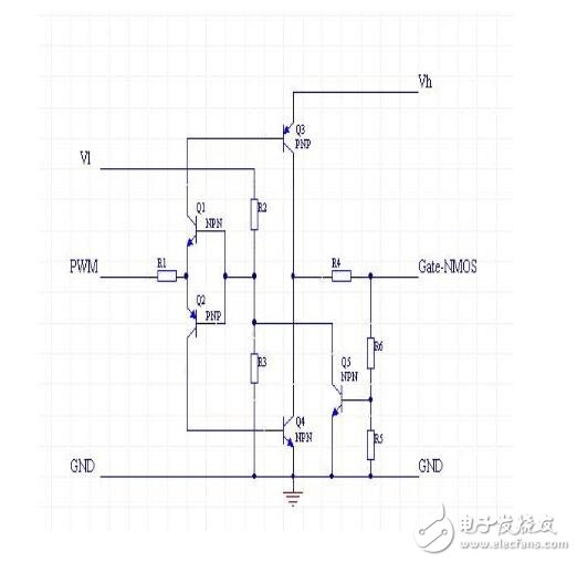
Figure 2 PMOS drive circuit
Here I only do a simple analysis for the NMOS driver circuit: Vl and Vh are low-side and high-side power supplies, respectively, and the two voltages can be the same, but Vl should not exceed Vh. Q1 and Q2 form an inverted totem pole for isolation, while ensuring that both drive tubes Q3 and Q4 are not conducting at the same time. R2 and R3 provide a PWM voltage reference. By changing this reference, the circuit can be operated in a position where the PWM signal waveform is steep. Q3 and Q4 are used to provide the drive current. Because of the conduction, Q3 and Q4 have only one Vce voltage drop relative to Vh and GND. This voltage drop is usually only about 0.3V, which is much lower than the Vce of 0.7V. R5 and R6 are feedback resistors that are used to sample the gate voltage. The sampled voltage produces a strong negative feedback on the bases of Q1 and Q2 through Q5, limiting the gate voltage to a finite value. This value can be adjusted by R5 and R6.
Finally, R1 provides a base current limit for Q3 and Q4, and R4 provides a gate current limit for MOS transistors, which is the limit for Ice for Q3 and Q4. Acceleration capacitors can be connected in parallel with R4 when necessary.
This circuit provides the following features:
1. Drive the high-end MOS transistor with low-side voltage and PWM.
2. Drive the MOS transistor with high gate voltage requirement with a small amplitude PWM signal.
3, the peak limit of the voltage of the gate
4, current limit of input and output
5. By using a suitable resistor, very low power consumption can be achieved.
6, the PWM signal is inverted. The NMOS does not require this feature and can be solved by pre-positioning an inverter.
When designing portable devices and wireless products, improving product performance and extending battery life are two issues designers face. The DC-DC converter has the advantages of high efficiency, large output current, and small quiescent current, making it ideal for powering portable devices. At present, the main trends in the development of DC-DC converter design technology are: (1) High-frequency technology: With the increase of switching frequency, the volume of the switching converter is also reduced, the power density is also greatly improved, and the dynamic response is improved. . The switching frequency of the low power DC-DC converter will rise to the megahertz level. (2) Low output voltage technology: With the continuous development of semiconductor manufacturing technology, the operating voltage of microprocessors and portable electronic devices is getting lower and lower, which requires future DC-DC converters to provide low output voltage to adapt to micro The requirements of processors and portable electronic devices, the development of these technologies put forward higher requirements for the design of power chip circuits.
First, as the switching frequency continues to increase, high requirements are placed on the performance of the switching elements, and corresponding switching element driving circuits must be provided to ensure that the switching elements operate normally at switching frequencies up to megahertz. Secondly, for battery-powered portable electronic devices, the operating voltage of the circuit is low (taking a lithium battery as an example, the operating voltage is 2.5 to 3.6 V), and therefore, the operating voltage of the power chip is low.
The MOS transistor has a very low on-resistance and consumes less energy. In the currently popular high-efficiency DC-DC chip, a MOS transistor is often used as a power switch. However, due to the large parasitic capacitance of the MOS transistor, the gate capacitance of the NMOS switch tube is generally as high as several tens of picofarads. This puts higher requirements on the design of the switching circuit of the high-frequency DC-DC converter.
In the low-voltage ULSI design, there are various CMOS, BiCMOS logic circuits using a bootstrap boost structure and a drive circuit as a large capacitive load. These circuits are capable of operating normally at voltages below 1V and can operate at frequencies of tens of megahertz or even hundreds of megahertz at load capacitances of 1 to 2 pF. This paper uses the bootstrap boost circuit to design a drive circuit with high load capacitance drive capability suitable for low voltage, high switching frequency step-up DC-DC converter. The circuit is based on the Samsung AHP615 BiCMOS process design and verified by Hspice simulation. When the supply voltage is 1.5V and the load capacitance is 60pF, the operating frequency can reach more than 5MHz.
Bootstrap boost circuit
The schematic diagram of the bootstrap boost circuit is shown in Figure 1. The so-called bootstrap boosting principle is to input a square wave signal at the input terminal IN, and use the capacitor Cboot to raise the voltage at point A to a level higher than VDD, so that the output terminal B can be inverted from the input signal and high. A square wave signal with a level higher than VDD. The specific working principle is as follows:
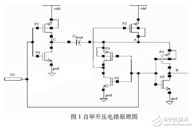
When VIN is high, the NMOS transistor N1 is turned on, the PMOS transistor P1 is turned off, and the potential at the C point is low. At the same time, N2 is turned on, and the gate potential of P2 is low, and P2 is turned on. This causes the potential at point A to be approximately VDD and the voltage across the capacitor Cboot to be UC ≈ VDD. Since N3 is turned on, P4 is turned off, so the potential at point B is low. This period of time is called the precharge cycle.
When VIN goes low, the NMOS transistor N1 is turned off, the PMOS transistor P1 is turned on, and the potential at the C point is high, which is about VDD. At the same time, N2 and N3 are cut off, and P3 is turned on. This causes the gate potential of P2 to rise and P2 to turn off. At this time, the potential at point A is equal to the potential at point C plus the voltage across the capacitor Cboot, which is about 2 VDD. Moreover, P4 is turned on, so point B outputs a high level and is higher than VDD. This period of time is called the bootstrap boost cycle.
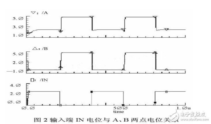
In fact, the potential at point B is related to the size of the load capacitor and capacitor Cboot, which can be adjusted according to the design needs. The specific relationship will be discussed in detail when introducing the specific design of the circuit. FIG. 2 is a schematic diagram showing the relationship between the potential of the input terminal IN and the potentials of the two points A and B.
Drive circuit structure
A circuit diagram of the drive circuit is shown in FIG. The driving circuit is designed by Totem output structure, and the pull-up driving tube is NMOS tube N4, transistor Q1 and PMOS tube P5. The pull-down drive transistor is an NMOS transistor N5. In the figure, CL is the load capacitance, and Cpar is the parasitic capacitance of point B. The circuit inside the dashed box is a bootstrap boost circuit.
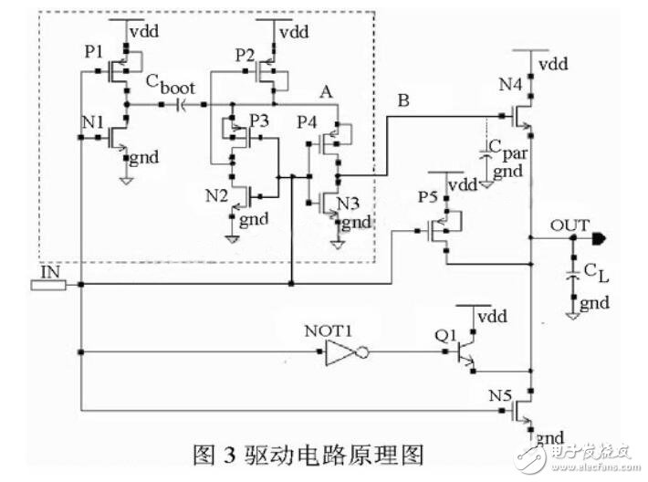
The design idea of ​​the driving circuit is to raise the potential of the gate (point B) of the pull-up driving transistor N4 by using the bootstrap boosting structure, so that UB>VDD+VTH, the NMOS transistor N4 operates in the linear region, so that the VDSN4 is greatly reduced. Small, the final drive output can reach VDD. When the output is low, the pull-down driver itself operates in the linear region, which ensures that the low-level bit GND is output. Therefore, the design requirements can be met without adding a bootstrap circuit.
Considering that the driving circuit is applied to the switching transistor driving of the step-up DC-DC converter, the load capacitance CL is large, generally can reach several tens of picofarads, and further needs to increase the output current capability, thereby increasing the transistor Q1 as a pull-up. Drive tube. Thus, when the input terminal changes from a high level to a low level, Q1 is turned on, and current is supplied by N4 and Q1 simultaneously, and the potential of the OUT terminal rises rapidly. When the potential of the OUT terminal rises to VDD-VBE, Q1 is turned off, and N4 continues to supply current. Charge the load capacitor until the OUT voltage reaches VDD.
During the high period at the OUT terminal, the potential at point A drops due to charge leakage on the capacitor Cboot. This causes the potential at point B to drop and the conductivity of N4 to decrease. At the same time, for the same reason, the potential at the OUT terminal will also drop, so that the output high level cannot be maintained at VDD. In order to prevent this phenomenon, the PMOS transistor P5 is added as a pull-up driving transistor to supplement the leakage charge of the OUT terminal CL, and the OUT terminal is maintained at a high level throughout the conduction period.
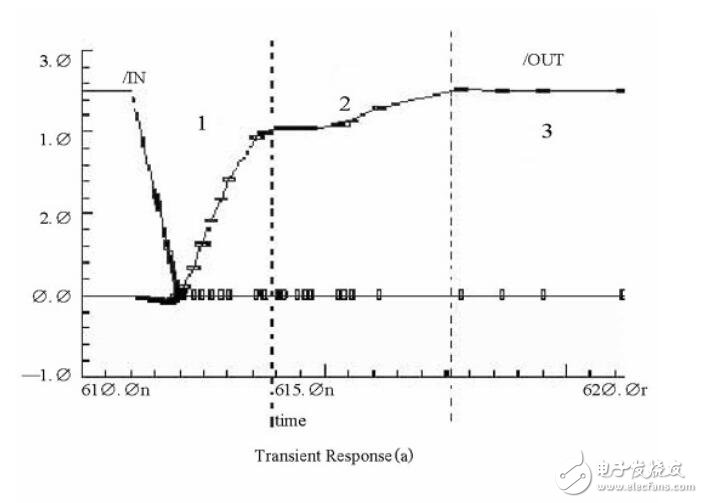
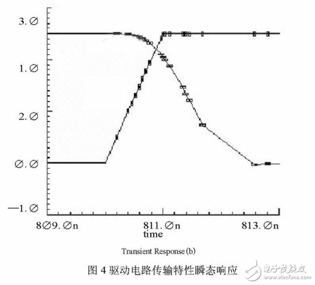
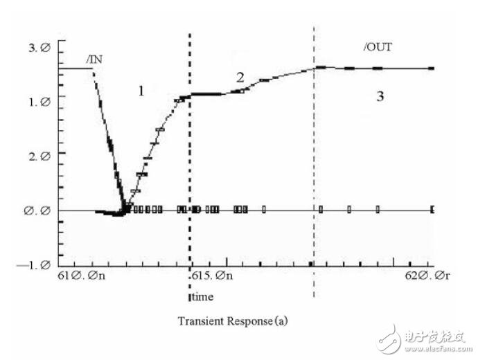
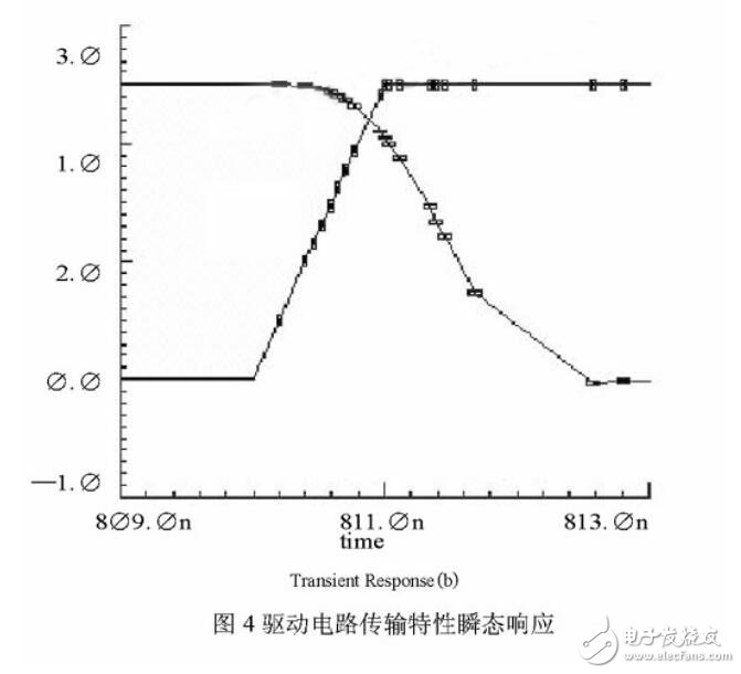
The transmission characteristic transient response of the drive circuit is given in Figure 4. Where (a) is the rising edge transient response and (b) is the falling edge transient response. It can be seen from Fig. 4 that the rising edge of the driving circuit is clearly divided into three parts, corresponding to the period in which the three pull-up driving tubes play a leading role. In the first stage, Q1 and N4 work together, and the output voltage rises rapidly. In the second stage, N4 plays the leading role, so that the output level reaches VDD. In the third stage, P5 plays a leading role, and the output high level is maintained as VDD. Moreover, the rise time can be shortened, and the fall time satisfies the requirement that the operating frequency is above the megahertz level.
Problems to be aware of and simulation results
Determination of the size of the capacitor Cboot
The minimum value of Cboot can be determined as follows. During the precharge cycle, the charge on capacitor Cboot is VDDCboot. The charge on the parasitic capacitance (calculated as CA) at point A is VDDCA. Therefore, during the precharge cycle, the total charge at point A is
Q_{A1}=V_{DD}C_{boot}+V_{DD}C_{A} (1)
The potential at point B is GND, so the charge on the parasitic capacitance Cpar at point B is zero.
In the bootstrap boost cycle, in order to bring the OUT terminal voltage to VDD, the potential at point B is at least VB = VDD + Vthn. Therefore, the charge on the parasitic capacitance Cpar at point B is
Q_{B}=(V_{DD}+V_{thn})Cpar (2)
Ignore the voltage drop across the source and drain of MOSFET P4. At this time, the charge on Cboot is VthnCboot, and the charge of parasitic capacitance CA at point A is (VDD+Vthn)CA. The total charge at point A is
QA2=V_{thn}C_{BOOT}+(V_{DD}+V_{thn})C_{A} (3)
At the same time, according to the conservation of charge
Q_{B}=Q_{A}-Q_{A2} (4)
Comprehensive formulas (1) to (4) are available
C_{boot}=\frac{V_{DD}+V_{thn}}{v_{DD}-v_{thn}}Cpar+\frac{v_{thn}}{v_{DD}-v_{thn}}C_ {A}=\frac{V_{B}}{v_{DD}-v_{thn}}Cpar+\frac{V_{thn}}{v_{DD}-v_{thn}}C_{A} (5)
As can be seen from the equation (5), the Cboot becomes larger as the input voltage becomes smaller, and becomes larger as the voltage VB at the point B becomes larger. The voltage at point B directly affects the on-resistance of N4, which also affects the rise time of the drive circuit. Therefore, in actual design, the value of Cboot is greater than the calculation result of equation (5), which can increase the voltage at point B, lower the on-resistance of N4, and reduce the rise time of the drive circuit.
P2, P4 size problem
After reorganizing formula (5):
V_{B}=({V_{DD}-V_{thn})\frac{C_{boot}}{Cpar}-V_{thn}\frac{C_{A}}{Cpar} (6)
It can be seen from equation (6) that during the bootstrap boost period, the parasitic capacitances of the two points A and B cause the potential at point B to decrease. In order to get the proper B point potential in actual design, in addition to increasing the Cboot size, the parasitic capacitance of the two points A and B should be minimized. At the time of design, the size of the precharge PMOS transistor P2 is as small as possible to reduce the parasitic capacitance CA. For the parasitic capacitance Cpar of point B, it is mainly the gate parasitic capacitance of the pull-up driving transistor N4, and the source-drain parasitic capacitance of the MOS transistors P4 and N3 is only a small part. In the previous analysis, we ignored the source-drain voltage of P4. Therefore, we should increase the P4 aspect ratio as much as possible so that the source-drain voltage during the bootstrap boost period is small. However, the size of P4 should not be too large, and it is necessary to ensure that the source parasitic capacitance of P4 is much smaller than the gate parasitic capacitance of pull-up drive transistor N4.
Well potential problem
As shown in FIG. 3, the N-wells of the PMOS devices P2, P3, and P4 are connected to the bootstrap boost node A. The purpose of this is to prevent their source/drain-well junctions from conducting during the bootstrap boost period. Moreover, it also prevents latch-up caused by parasitic SRC when the source/drain-well is positively biased.
The well bias potential of the pull-up driver N4 is connected to its source, preferably not directly to ground. The purpose of this is to eliminate the effect of the substrate bias effect on N4.
Hspice simulation verification results
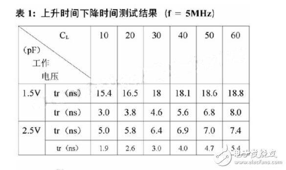
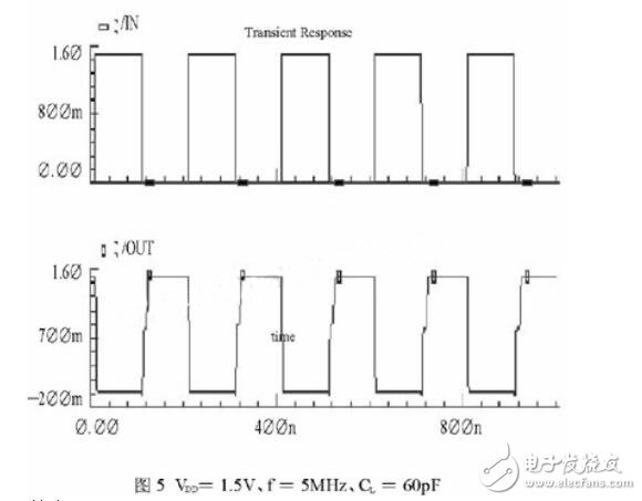
The driver circuit is based on the Samsung AHP615 BiCMOS process design and verified by Hspice simulation. The simulation results of the rise time tr and the fall time tf of the circuit under different operating voltages and different load conditions are given in Table 1. In Figure 5, the output waveform of the circuit operating at an input voltage of 1.5V, an operating frequency of 5MHz, and a load capacitance of 60pF is given.
As can be seen from Table 1 and Figure 5, the driver circuit can operate normally with an operating voltage of 1.5V, an operating frequency of 5MHz, and a load capacitance of up to 60pF. It can be applied to a driving circuit of a switching tube in a low-voltage, high-frequency DC-DC converter.
Conclusion In this paper, the bootstrap circuit, a drive circuit is designed BiCMOS Totem structure. The circuit is based on the Samsung AHP615 BiCMOS process and operates under 1.5V supply conditions, and operates at frequencies up to 5MHz with a load capacitance of 60pF.
XB2-B Series Pushbutton Switch
XB2-B series Pushbutton Switch are using controlling circuit of AC voltage up to 660V/AC 50Hz.and DC voltage below 400V.It is used for controlling signal and interlocking purposes.The main body of the push buttons adopts Circuit head,with chromium plated metal bezel,Complete units with screw and captive cable clamp connections.The contact adopts special silver alloy in order to enjoy the benefit of high anti-electrical erosion.The signal lamp series are suitable for electrical applicances circuit of AC voltage up to 380V/50Hz,and DC voltage below 380V.It is ideal for using as indicating signals,warning signals,emergency signals.

Push Button On Off Switch,Waterproof Push Button Switch,Micro Push Button On Off Switch,Green Push Button Switch
Ningbo Bond Industrial Electric Co., Ltd. , https://www.bondelectro.com