This article focuses on the experimental testing of the THS4271 operational amplifier from Texas Instruments (TI). The circuit was designed to evaluate key parameters such as input offset voltage, input offset current, common-mode rejection ratio (CMRR), and open-loop differential gain. These measurements were conducted under controlled conditions to ensure accuracy and reliability. The results provide a comprehensive understanding of the device's performance and its suitability for various applications.
The THS4271 is known for its low noise, high slew rate, and unity-gain stability, making it an ideal choice for high-performance analog circuits. Its wide operating voltage range (5V to 15V) allows flexibility in different system designs. The amplifier also features a wide bandwidth and low distortion, which are crucial for maintaining signal integrity in complex applications.
Throughout this study, several practical examples were explored to demonstrate how the THS4271 can be effectively used in real-world engineering scenarios. These examples highlight the amplifier’s versatility and its ability to meet demanding performance requirements in modern electronic systems.
Despite the advancements in integrated circuit technology, operational amplifiers remain essential components in many applications. As a result, ongoing research into high-performance op amps continues to be vital. This paper not only presents the measured characteristics of the THS4271 but also discusses their implications for future development and user applications.
1. Chip Introduction
The THS4271 is a high-performance voltage feedback amplifier manufactured by TI. It is designed for applications requiring low noise, high slew rate, and excellent stability. The device operates within a supply voltage range of 5V to 15V and offers a wide bandwidth, low distortion, and a high dynamic range. This makes it suitable for use in a variety of high-precision analog systems.
The THS4271 is available in multiple package options, including SOIC, MSOP with PowerPAD, and leadless MSOP with PowerPAD. These packaging choices allow for flexible integration into different types of circuits. Table 1 outlines some of the key specifications of the THS4271.
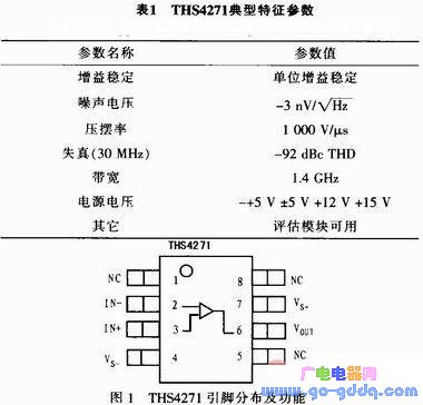
The physical layout and pin configuration of the THS4271 are shown in Figure 1. Each pin has a specific function, and some are marked as "NC," meaning they are not connected.
2. Experimental Principle
2.1 Input Offset Voltage
In an ideal operational amplifier, the output should be zero when the input is zero. However, due to internal asymmetry, the actual output may not be zero without external compensation. This deviation is known as the input offset voltage (UIO). A small UIO value indicates better symmetry and higher performance.
2.2 Input Offset Current
The input offset current (IIO) refers to the difference between the bias currents at the two inputs of the op amp. A lower IIO means less impact on the output DC level, especially in high-impedance signal sources.
2.3 Common-Mode Rejection Ratio (CMRR)
The CMRR measures the amplifier's ability to reject common-mode signals. A higher CMRR indicates better immunity to interference and improved circuit symmetry.
2.4 Open-Loop Differential Gain
This parameter represents the gain of the op amp without any feedback. It is calculated as the ratio of the output voltage to the differential input voltage. A higher open-loop gain contributes to better overall performance.
3. Test Circuit, Data, and Analysis
3.1 Measurement of Input Offset Voltage
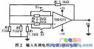
A schematic diagram of the offset voltage test circuit is shown in Figure 2. By closing switches S1 and S2 and shorting resistor Ra, the output voltage was measured. Using the formula UIO = R1 * UO / (R1 + Rf), the input offset voltage was calculated as 3.85 mV, based on an output voltage of 385 mV.
Charger for laptop,
FOSHAN SHUNDE KELICHENG POWER SUPPLY TECHNOLOGY CO., LTD , https://www.kelicpower.com