FPGA (Field-Programmable Gate Array), Field Programmable Gate Array, is the product of further development based on PAL, GAL, CPLD and other programmable devices. It appears as a kind of semi-custom circuit in the application-specific integrated circuit (ASIC) field, which not only solves the defect of the custom circuit, but also overcomes the shortcomings of the original programmable device with a limited number of gates.
This article mainly introduces the on-chip resource usage of FPGAs, which are detailed analysis from combinational logic and sequential logic.
How to analyze the utilization of combinational logic (LUT) and sequential logic (REG) on the FPGA chip.
First, how to get the proportion of LUT and REG use
Let's first look at a compilation report of an FPGA project:
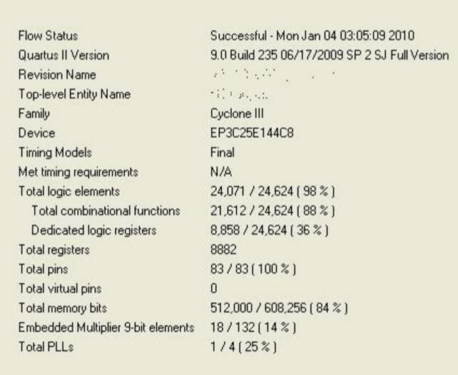
In this report, we can see the following information:
Total logic elements 24071/24624 (98%): There are 24,624 LE resources in this chip, 98% of which are used in this compilation of this project.
Total combinaTIonal funcTIons 21612/24624 (88%): Of the 24,624 LE resources of the chip, 88% were used to implement combinatorial logic.
Dedicated logic registers 8858/24624 (36%): Of the 24,624 LE resources of the chip, 36% are used to implement registers, ie, sequential logic.
From the above information, I got the ratio of the use of combinational logic and sequential logic - 21612/8858 = 2.4:1.
Second, a more detailed resource utilization report
In this report, one thing may be confusing: why the sum of Total combinaTIonal funcTIons and Dedicated logic registers (30470) is greater than Total logic elements (24071), and even greater than the chip's total resources (24624). Let's look at a more detailed resource use report - Fitter Resource Usage Summary:
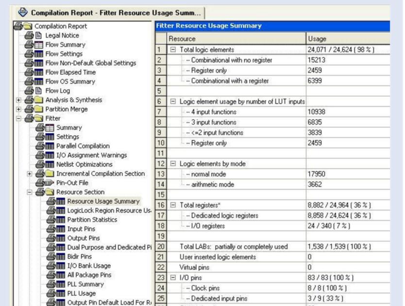
This report contains a lot of information. Here we only need to care about Total logic elements. Total logic elements 24071/24624 (98%) consists of three LE resources with different use cases: LE (Combinational with no register 15213) only for implementing combinatorial logic, LE only for implementing temporal logic (Register only 2459) , Also used to implement combinational and sequential logic LE (Combinational with a register 6399).
Third, from the Resource Property Editor to see the use of LE
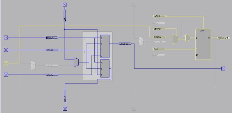
Before further analyzing these data, it is necessary to review the structure and function of the basic element LE (Logic Element) of the FPGA. Take Altera's Cyclone III series FPGA chip as an example, the internal structure of LE is shown in the following figure:
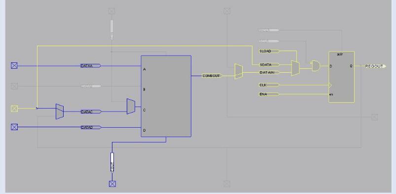
This LE is also used to implement combinatorial logic and sequential logic, where the blue part is the combinatorial logic (a 4-input LUT), where the yellow highlighted part is the timing logic (a D flip-flop). Let's look at a more interesting LE:
This LE is also used to implement combinational logic and sequential logic. The difference from the previous figure is that the combinational logic (4-input LUT) does not have a connection relation with the sequential logic (REG). The combinational logic is output directly from COMBOUT and the timing logic is output from REGOUT. This kind of irrelevant combinatorial logic and timing logic sharing the same LE is very special, this is the implementation of the use of the Register Packing resource optimization technology. If this resource optimization technique is not used, two LEs are used to implement the corresponding combinational logic and sequential logic, respectively.
Understand the above two figures, we can also be analogous to this, imagine LE (Combinational with no register) only used to achieve combinational logic and LE (Register only) only used to implement sequential logic.
Fourth, "The numbers are finally on!"
Let's go back to the previous section on resource utilization analysis. With the knowledge described above, everyone should be able to distinguish between three different LEs in the resource utilization report.
We add "LE (6399), which is used to implement combinatorial logic and sequential logic at the same time," to "LE (15213), which is only used to implement combinatorial logic," and "LE (2459), which is only used to implement sequential logic." You can get two values ​​of "Total combinatorial logic functions" (Total combinational functions = 6399 + 15213 = 21612) and "Dedicated logic registers = 6399 + 2459 = 8858". These two values ​​are the results of the summary report on resource utilization in the first figure, and their proportion is exactly 2.4:1.
Since the 6399 number was used twice, we originally stated that the sum of "Total combinational functions and Dedicated logic registers (30470 = (6399 + 15213) + (6399 + 2459)) is greater than Total logic elements (24071 = 6399 + 15213 + The puzzle of 2459) was also answered.
V. Summary
Because the number of combinatorial logic and sequential logic used in the FPGA design is not balanced, some LEs will only be used to implement combinatorial logic or sequential logic; further, due to the limitations of layout location, the two LEs that implement combinatorial logic or sequential logic alone may be Cannot be combined into an LE implementation. Therefore, there will be three different LEs in the resource utilization report.
Since long combinatorial logic chains (cascaded LUTs) introduce large delays, sequential logic (REG) can split longer combinatorial logic chains into shorter combinatorial logic chains, effectively shortening the critical path and The length of the secondary critical path, in turn, improves the overall timing performance of the FPGA design, so the use of combinational logic and sequential logic can be used as an auxiliary parameter to evaluate the timing performance of an FPGA design.
Overly complex combinatorial logic also consumes multiple LEs. When we write HDL code, we can not reduce the amount of use of Register as a means of saving resources, but should take into account the combination of logic and sequential logic, according to the underlying structure of the target PLD device, writing combinational logic and timing logic ratio in line with PLD device resources The proportion of the code.
Iget bar flavours has 13 differentce, the flavor of the iget bar is amazing and exotic, you can enjoy different flavours from Mango ice, blueberry ice to double apple etc. it's the upgrade vape in the iget brand vape, The main market is Australia, USA, Russia etc. The design of the iget bar incorporates Chinese elements, so it looks very nice and comfortable. With the large capacity of 12ml e-liquid and strong power of 1500Mah battery, the iget bar puffs is up to 3500puffs, which is double puffs compare to IGET Xxl! It seems it can work forever! The nic salt is 5%, apply for the vaping person demanded for the nic strength.
For the Iget Vape, besides iget bar 3500, there are iget legend, iget xxl 1800, iget shion, iget king, iget max and others, all of them are original that you can buy them without worried to buy a fake iget vape.
Iget Bar vape, iget bar flavours, iget bar 3500, iget bar vapes, iget bar price, iget bar puffs
Shenzhen Kate Technology Co., Ltd. , http://www.katevape.com