Xiang Hao, Li Mu, Hager Communications
Keywords: OpenVPX, VPX backplane, broadband switching, RapidIO, PCIe
The VPX bus is a new generation of high-speed serial bus standard proposed by VITA (VME International Trade Association) in 2007 based on its VME bus. The basic specifications, mechanical structure, and bus signals of the VPX bus are defined in the VITA46 series technical specifications. The VPX bus introduced the latest serial bus technologies (such as RapidIO, PCI-Express, and 10 Gigabit Ethernet) to replace the original parallel bus technology and support higher backplane bandwidth.
At present, most military switching equipment use custom parallel buses, which have low bandwidth and poor scalability. Each manufacturer's equipment and board cards are incompatible. All functions need to be developed by themselves. The product development cycle is long and the production and maintenance costs are high. OpenVPX is currently the only computer standard system for military and aerospace and other high-level security areas. The application of OpenVPX to the military broadband switching platform is an inevitable trend of technology development.
1 Broadband Switching Platform Design
The broadband switching platform equipment is a standard 19-inch upper rack equipment with a height of 4U and air cooling. Including backplane, fan board, power module, switch module, load module and RTM (Rear Transition Module) module. The device goes out through the RTM. The front view of the broadband switching platform is shown in Figure 1.
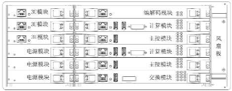
Figure 1 Front view of broadband switching platform
The backplane supports six 6U front/rear insertion module slots, three 3U front/rear insertion module slots, one fan slot, and three 3U VPX power supply slots. Except the exchange slots, other 3U/6U slots can be mixed before and after. The whole Machine not only supports 6U VPX modules, but also supports 3U VPX modules, providing flexible options for applications of different sizes. The fan board is equipped with four 3.24W fans with a rated air flow of 30.7CFM. The fans support PWM speed control, blows from the right side to the left, and dissipates heat for the front board. There is no key device in the rear board area and no heat dissipation is required.
The complete machine supports up to three power modules. The single power module has a rated power of 200W and supports main power 12V, 3.3V, and 5V current sharing. According to the actual number of service boards, the number of power modules can be flexibly increased or decreased.
2 backplane design
VITA65 defines the following terms in section 1.3.2 to describe the data channel width:
UTP (Ultra-Thin Pipe): A 1x link width, a communication channel consisting of a pair of differential transmission signals and a pair of differential reception signals.
TP (Thin Pipe): It is a link width of 2x and consists of two pairs of differential transmission signals and one pair of differential reception signals.
FP (Fat Pipe): A 4x link width, a communication channel consisting of 4 pairs of differential transmission signals and 4 pairs of differential reception signals.
The backplane adds 3U expansion slots to the 6U standard slot, allowing 3U load modules and RTMs to be inserted.
The VITA65 logically divides the data transmission channels in the system into CP (Control Plane), DP (Data Plane), EP (Expansion Plane), Management Plane, and Common Plane ( Utility Plane). The control plane is used to transmit device control information; the data plane is used to transmit high-throughput, real-time data at the application layer; the expansion plane is used for data transmission between the master and slave devices in adjacent slots; and the management plane is used for the Intelligent Platform Management Bus (IPMB). Out-of-band information transmission channel; common plane includes power supply, reset, clock, slot number, JTAG, and other spurious signals.
The control plane, data plane, and expansion plane of the backplane do not specify the type of bus protocol. What protocol these planes transmit is defined in the switch module and the load module, which adds more flexibility to the system. The topology of the backplane is shown in Figure 2, and described in connection with Figure 4:
Control plane: CPUtp1, CPUtp2 (UTP, two 1x chain widths) of each load slot located on the J4 connector are respectively connected to the switching slot UTP1-16. The switch module provides 16 GEs and works in 1000BASE-X mode. It forms a star-switched network with each board.
Data plane: DP01 (FP, 4x chain width) of each load slot located on the J1 connector is connected to the switch slot DP8-DP12. At the same time, DP3 of each load slot is connected to the left slot DP4, and DP4 of each load slot is connected to DP3 of the right slot. The switch module provides SRIO or PCIe switch links through the XMC daughter card.
Expansion plane: Each load slot is located at EP0-7 (DFP, 8x chain width) of the J2 connector, and EP8-15 (DFP) is connected to J2 of two adjacent slots. If the computing module provides SATA interfaces to the adjacent slots, the adjacent slots can be configured with storage modules.
Management plane: The backplane provides 1 bus and 1 bus and 2 bus-type I2C channels for out-of-band communication between the switch module and each load module to perform system management such as power-on and power-off and temperature control.
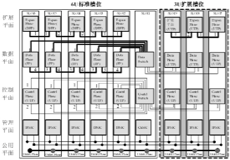
Figure 2 Backplane bus topology
3 core board design
OpenVPX defines switch module (SWITCH), load module (PAYLOAD), peripheral module (Peripheral) and storage module (STORAGE) module types. In this exchange platform, the first two modules are used: the exchange module and the load module (such as the calculation module, the main control module, the codec module, etc.). In order to minimize the type of module maintenance and reduce system maintenance costs, a compatible design was implemented in the switch module. When the switch module is inserted into the load slot, it can work in the load module mode. Exchange module block diagram shown in Figure 3.
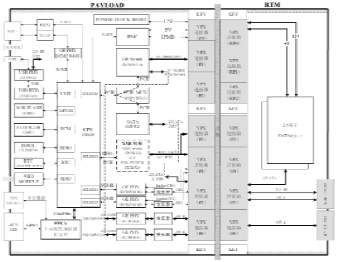
Figure 3 Switch Module Block Diagram
3.1 Switch Module and Load Module Definition
VITA65 defines the exchange model SLT6-SWH-16U20F-10.4.2 in Section 10.4.1; Load Model SLT6-PAY-4F1Q2U2T-10.2.1 is defined in Section 10.2.1. The definition of the switching module and the load module in this platform fully complies with the above definition. As shown in Figure 4, where Pn represents the corresponding module plug, Jn represents the corresponding backplane socket.
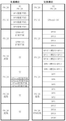
Figure 4 module signal definition
3.2 Exchange Module CPU Small System
The CPU selected for the switch module is the P2020. The P2020 is Freescale's QorIQ P2 platform product that enables single-thread, high-performance, power-ratio to be used in a variety of applications in the telecommunications, military, and industrial fields. On the 45nm technology low-power platform, this series of products can achieve 1.2GHz dual-core frequency. QorIQ P2 series consists of dual-core and single-core products. These products are pin-compatible with QorIQ P1 platform products and are fully compatible with software. They provide a set of five interchangeable cost-effective solutions that can be based on actual computing power. Requirements, mounting different CPUs on the same PCB to meet a variety of user needs.
The QorIQ P2 series integrates four SerDes channels that can be allocated between two serial RapidIO ports, three PCI Express ports, and two SGMII ports. The four SerDes channels can be flexibly changed by the software configuration.
The switch module CPU hardware configuration is as follows:
CPU: P2020, 1.2GHz, dual-core, can be replaced with P1020, P1021, etc.;
Memory: DDR3L, 2GB, use low-voltage memory particles, Vcc = 1.35V, power consumption is lower than 1.5V DDR3.
Storage: NOR Flash 16MB, used to store uboot, embedded Linux operating system kernel, application programs and configuration information; NAND Flash 2GB, used to store business data.
Serial port: 1 debug serial port for board debugging command input and information display; another serial port is connected to IPMI module for board management.
Network port: One Fast Ethernet debugging network port for board debugging and program loading; Two Gigabit Ethernet ports (SerDes2/3 working in SGMII mode), outgoing to BCM54616S, P5/J5 to RTM modules, for Intercept packets in the network.
Wi-Fi: The CPU connects to the Wi-Fi module through the SDIO interface. The mobile terminal device can configure and manage the broadband switching platform through WIFI access.
SATA: 2-way SATA 2.0 interface, connected to the SATA hard disk socket on the RTM module through P5/J5. The switch module has 2GB NAND Flash installed onboard, and it can install SATA hard disks on RTM when capacity is insufficient.
PCIe interface: one, through the PCIe selection switch, and 24 port Gigabit switching chip BCM56334 connection; work in the load module mode, and SATA conversion chip connection.
SRIO interface: SerDes1 can be configured in SRIO mode and connected to the SRIO switch chip CPS1616 of the XMC daughter board. It can also be configured as a PCIe interface and connected to the PCIe switch chip PEX8524 of the XMC daughter board.
3.3 Switching Module Control Plane Switching Subsystem
The control plane switching chip selects BROADCOM's 24-port three-layer Gigabit Ethernet switch chip BCM56334. The CPU initializes and configures the BCM56334 through the PCIe interface to send and receive data packets. The BCM56334 provides 24 SerDes interfaces that can operate in SGMII mode or 1000BASE. -X mode.
In the switch module, the 8-way SerDes operates in SGMII mode, and an external two 4-port PHY chip is provided. After the transformer and P5/J5 and RTM, eight three-level Gigabit Ethernet interfaces are provided externally. The other 16 SerDes work in 1000BASE-X mode, support 64B/66B codec function, no external PHY, directly through the P1/J1 on the backplane bus, and the load slot control plane CPU communication. The backplane has five 6U load slots, three 3U expansion slots, and two 1000BASE-X slots in each slot.
3.4 Switch Module Data Plane Switching Subsystem
The protocol of the broadband switching platform data plane can be either SRIO or PCIe. To increase system flexibility, you can install XMC daughter boards of different types (such as PCIe switches or SRIO switches) on the switch module carrier board. The XMC daughter card is a standard card that complies with the VITA42.0 specification. VITA42.2 defines the definition of the SRIO protocol on the XMC connector. VITA42.3 specifies the definition of the PCIe protocol on the XMC connector.
Supporting the SRIO protocol XMC pinch board, IDT's SRIO switch chip CPS1616 is used to flexibly configure four x4 or eight x2 or 16 x1 ports. There are a total of 5 6U service slots in the broadband switching platform. The link bandwidth is allocated as follows: 2x4, 3x2, 1x1 CPUs with 1x1 switch modules, 1x1 reserved.
The PCIe protocol-capable XMC daughter card uses PEX's PCIe switching chip PEX8524, which can be flexibly configured as six x4 or six x2 ports. Each 6U slot in the broadband switching platform is assigned a data plane channel of x4 chain width, and a x4 CPU of the switching module.
In addition, a data plane with an x4 chain width is reserved for each of the two adjacent slots on the left and right sides of the data plane. The data plane can be used for concatenation of DSPs or CPUs in adjacent slots to provide signal processing or computing capabilities.
3.5 Switching between Switch Module and Load Module
When the switching module in the broadband switching platform is inserted into the load slot, it can switch to the working mode of the load module. The load module needs to provide two x1 UTP control plane channels on the P4 connector.
The BCM54616S implements SGMII to coper or SGMII to SerDes functions. By configuring the automatic media identification register (address 0x1C) of the BCM54616S, it is possible to switch between the above two modes. The exchange slot indicator signal SYS_CON is pulled low on the backplane and floated in other load slots. The module can identify the current slot type by detecting this signal. If the signal is low, the BCM54616S is automatically configured in the SGMII to coper mode; otherwise it is configured in the SGMII to SerDes mode, ie, the SerDes2/3 of the CPU (operating in the SGMII mode) through the BCM54616 It is converted to 2-way 1000BASE-X upper back as the control plane channel of the load module.
4 System Reliability Design
The complete line of the aircraft adopts a high-reliability avionics connector that meets the requirements of the national military standard. The surface is plated with bright nickel and the shell is conductive.
Since the RTM module needs to be inserted from the back of the chassis and the outlet of the entire machine is behind the chassis, if the RTM module fails, it is inconvenient to replace and repair the RTM module. In order to increase the reliability of the RTM module as much as possible, all the core devices are laid out on the front board, and only the wiring and the necessary decoupling capacitors are placed on the RTM module. Through long-term reliability testing, the RTM module has never failed.
5 Concluding remarks
This article applies the VPX technology to the military broadband switching platform and improves the system bandwidth. Through standardized modular design, device interoperability between various vendors is enhanced; mature modules can be directly inserted into the system for use and shortened. New product development cycle. Through the compatible design of the module, the hardware cost is further reduced.
The positioning of VPX is oriented to the harsh areas of the working environment such as military and aerospace, and has not been used on a large scale in the civilian sector. The RT2 series of backplane connectors currently rely mainly on imports, which has a high cost. With the gradual localization of RT2 connectors, connector costs will gradually decrease, which will further promote the application of VPX in military communications equipment.
The bus speed supported by the VPX is high. As the power density of the cell module increases, the design of the entire device needs to focus on the heat dissipation problem. By designing a reasonable air duct, introducing a conduction cooling standard that conforms to VITA 48.2, introducing liquid-cooled heat dissipation, and even comprehensively using these three heat-dissipation methods, it is the research direction for future machine design.
PCD Inserts
PCD Inserts
OPT Cutting Tools Co., Ltd specialize in offering a comprehensive gamut of PCD diamond inserts, Some of our major product include PCD milling inserts and PCD turning inserts. Then, how to identify the different of them?
Turning is machining that is generally conducted on a lathe. To make it easier to comprehend turning, imagine the machining of a car shaft for example. The workpiece is held by both ends and rotated. Then a tool on a tool post or, if manual, held by hand is moved into the workpiece to carry out the machining.


Milling is opposite to that of turning.(major product: pcd inserts PCD cutting inserts PCD Milling Inserts PCD Grooving Inserts) When milling the workpiece is stationary and the tool is rotated. As the tool rotates one or more of the cutting edges engages with the workpiece and removes material. Therefore due to the action of the cutting edges coming into and out of contact with the workpiece the machining is interrupted machining. As the cutting edges engage and disengage with the workpiece the cutting edges are subjected to severe thermal shock. This is due to the rapid temperatures increase due to friction during the cut and rapid cooling as this cutting edge disengages from the workpiece. Therefore, to enable and achieve highefficiency machining, cutting tool manufacturers strive to improve and develop tool materials and cutting edge geometries. For milling, it is important to select a tool grade material that can withstand severe working conditions and a cutting edge geometry that can maximize the performance of the cutter.
Generally, PCD inserts are identified by different geometry by using letters of the alphabet. A wide range of geometries are listed as standard, Here we present some of PCD diamond inserts which widely used.
PRODUCT DETAIL:


product catagory :

PRODUCTING PROGRESS:

PAYMENT AND DELIVERY:

PRODUCT EQUIPMENT :

ABOUT US :
We are specialize in manufacturing PCD diamond tools and Carbide tools. Our major product inclulde PCD inserts, PCD Reamers , PCD End Mills, PCD Taps, Cabide Inserts,Carbide Drills, Carbide Reams, Taps etc.,
we also offered customized cutting tools per drawings, and provide package according to customer requirements. We manufacture a series range of cutting tools for machining of Cast iron, Aluminium alloy and Non-Ferros metal, it is widely used in all major sectors like Automobiles, Engineering, Aerospace, Aviation and 3C industry. Premium quality of raw material is used in the production and strict examination during processing with advanced equipment, so our client are satisfied with our reliable quality and on-time delivery.
Our best selling of cutting tools include PCD Inserts, PCD End Mill, PCD Ball Nose Mill, PCD Reamer, Carbide Taps , Carbide End Mill, Special Form Cutter and many more. For these years we have been made a large forward in the technologies of manufacturing cutting tools. With high quality on performance and price, our product sells well both on domestic and overseas market. And we will always focus on the quality and best service, to make long business relationship.

quanlity control:
We have dedicated team of quality control and precise equipment to keep good and stable performance for our products and processing services.

Chip Breaker,PCD Indexable Inserts,Diamond Blade,PCD Chipbreaker Groove Blade
OPT Cutting Tools Co., Ltd. , https://www.optdiamondtoolss.com