In reality, there is a need for a boost DC power supply that can convert a lower DC voltage into a higher output voltage and allow a larger current output. The power supply circuit is facing small power consumption, stable output voltage, small size, light weight, high conversion efficiency, energy saving and other aspects. This paper is based on xl6009 design switching boost power supply with the above advantages, and has certain practical value.
2, circuit design ideasBased on the xl6009 switching boost power supply, the principle block diagram is shown in Figure 1. The DC power output 24V voltage is sent to two switch boost power modules based on xl6009 design, and the two switch boost power supplies will send 24V respectively. The DC voltage rises to an output voltage of 36V to supply power to the same carrier. In order to improve the performance of the power supply, especially to ensure that the power supply has a large output power, two boost modules are used in parallel to supply power to the load. The ratio of the current supplied by the two power modules to the load is set to 1:1, and the ratio of the supply current can be achieved by fine-tuning the output voltage of the boost module.
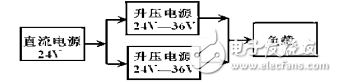
Figure 1 is based on the XL6009 step-up switching regulator power supply block diagram
3, chip X6L009 introductionThe internal structure of the chip XL6009 is shown in Figure 2. The pin diagram of the chip xL6009 is shown in Figure 3. 1 pin is the ground terminal; 2 pin is the enable terminal (high level output voltage, low level can not output voltage); 3 pin is the switch signal output terminal; 4 pin is the input terminal; 5 pin is the feedback terminal.
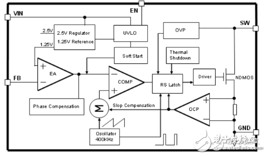
Figure 2 Internal structure of XL6009
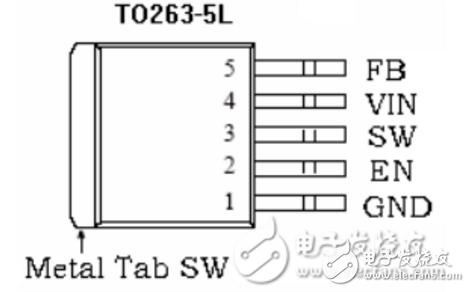
Figure 3xL6009 pin diagram
The chip x16009 regulator is a wide input range, current mode, DC/DC converter capable of generating positive or negative output voltage. It can be configured as a boost flyback SEPIC or inverting converter.
The chip x16009 consists of a power N-channel MosFET tube and a fixed frequency oscillator. The current mode structure operates stably over a wide range of input and output voltages. Features of the chip x16009 regulator:
(1) Input voltage range v5 to 32v;
(2) Use a feedback pin to set the output voltage to positive or negative;
(3) Current mode control provides excellent transient response;
(4) 1.2v5 reference voltage adjustable mode;
(5) Fixed a switching frequency of 400 kHz;
(6) Maximum 4A switching current;
(7) The sw pin implements overvoltage protection;
(8) The efficiency is as high as 94 degrees.
Etching cutting die is mainly used in the die-cutting industry to cut product labels. Generally applied to trademarks, printing and packaging, various paper art, fabric creation, home beautification, office decoration, double-sided adhesive, single-sided adhesive, stickers and more.
The main characteristics of the die cuts are that it has no jointing, high precision and a higher service life than laser cutting dies. The size of the product is stable during the die-cutting process, the maintenance requirements are simple during the storage of the moulds, and long-term storage will not affect the size of the product.
We customize diverse patterns Mould products with drawings provided by customers. We are equipped with professional metal etching equipment and exposure development equipment. The accuracy of our moulds can be maintained at ±0.05mm, the material uses is high hardness 65 Mn Steel. We can guarantee that our hard mould cutting die have straight blade lines, consistent width and height, as well as the blade height and bottom thickness accuracy also meet the customer's requirements.
Hard Mould Cutting Die,Diverse Patterns Mould, High Hardness 65 Mn Steel,Die cuts
SHAOXING HUALI ELECTRONICS CO., LTD. , https://www.cnsxhuali.com