A similar article was also published in Maxim Engineering Journal, Issue 64 (PDF, 2.5MB). Overview White LED (WLED) has a small form factor and high brightness output. It is an ideal backlight solution for small-sized color displays in mobile phones and other portable devices. However, WLEDs used in single-cell lithium-ion (Li +) battery-powered devices often encounter a problem. The operating voltage of most Li + batteries is 3V to 4.2V, while the forward voltage of WLED is usually 3.5V to 3.8V (at a current of 20mA). Therefore, the low voltage side of the operating voltage range of the Li + battery cannot meet the requirements of the WLED bias voltage.
The following two methods are usually used to generate sufficient WLED forward bias voltage: capacitive charge pump and inductor-based boost circuit. Considering efficiency and battery life, inductance-based circuits are usually the best choice. However, such circuits require additional expensive inductance and must be carefully laid out and designed to avoid electromagnetic and radio frequency interference. In contrast, charge pump schemes are easy to implement and low in cost, but they tend to be less efficient, thus reducing battery operating time accordingly.
Negative charge pump technology provides a low-cost, high-efficiency solution Maxim's negative charge pump architecture has an adaptive switching function that can achieve the efficiency of an inductive architecture (average efficiency is 85%), while retaining the simplicity and low cost of an inductorless design And other advantages.
This innovative architecture uses an adaptive switching mode to provide independent power supply, dimming and current regulation for each LED, which increases the LED drive efficiency by 12%, which can effectively extend battery life and save PCB space in portable products. Because it can achieve the same conversion efficiency as the inductor design, the energy efficiency of the system is greatly improved.
The efficiency of the fractional charge pump is improved. The core of the first generation WLED charge pump solution uses a basic voltage double topology (or 2 voltage double mode). The efficiency of a 2x voltage charge pump is: PLED / PIN = VLED × ILED / [(2 × VIN × ILED + IQ × ​​VIN)] where IQ is the static operating current of the circuit.
Because IQ is often small compared to WLED load current, the efficiency can be approximated as: PLED / PIN ≈ VLED / 2VIN In order to improve efficiency, the output of the second-generation WLED charge pump is not always an integer multiple of the input. If the battery voltage is not enough, a 1.5-fold charge pump will be used to generate a sufficiently high WLED drive voltage. The conversion efficiency of the 1.5 times charge pump is: PLED / PIN = VLED × ILED / (1.5 × VIN × ILED + IQ × ​​VIN)
The third-generation WLED driver adds a 1x voltage mode. In this mode, when the battery voltage is high, the battery is directly connected to the LED through the low-dropout current regulator. The efficiency in 1x voltage mode is: PLED / PIN = VLED × ILED / (VIN × ILED + IQ × ​​VIN)
The WLED driver design that improves efficiency at any battery voltage provides the most efficient power transfer mode for a given battery voltage and LED voltage. As the battery (or WLED) voltage changes, the design will change the mode accordingly. However, when the battery voltage is higher, switching losses will reduce efficiency, and these losses are often unnecessary. When the battery voltage drops, the driver should be in high efficiency mode for as long as possible. However, this requires reducing the loss of the power switch as much as possible, correspondingly taking up more space, and the cost will increase accordingly.
As described above, the 1x voltage transmission mode has the highest efficiency, but this mode is only applicable to the case where the battery voltage is higher than the WLED forward voltage (VF). The key to adopting the double voltage mode in applications where the battery voltage is as low as possible is often to reduce the voltage drop of the bypass FET and current regulator in the double voltage mode. These voltage drops often determine the series losses and the minimum input voltage required to maintain 1x voltage mode. The minimum battery voltage required for 1x voltage mode is equal to:
VIN (MIN_1X) = VLED + RDS (ON) of the bypass pFET × (ILED + VDROPOUT of the current regulator) The traditional positive charge pump WLED scheme uses a pFET bypass switch to connect the battery voltage to the WLED, as shown in Figure 1. The RDS (ON) of this FET is usually 1Ω to 2Ω. Further reduction in resistance is often limited, because lower resistance often requires larger FETs, which increases the cost of power devices.
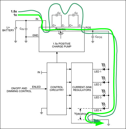
Figure 1. In 1x voltage mode, the positive charge pump uses an internal switch to bypass VIN to the WLED anode.
When VIN cannot meet the requirements of the 1x voltage transfer mode, the positive charge pump generates 1.5x VIN or 2x VIN to drive the anode of the WLED. When implementing 1x voltage mode in a positive charge pump architecture, an additional internal switch must be used to connect VIN directly to the anode of the WLED, thereby bypassing the charge pump.
When VIN cannot drive WLED, the negative charge pump structure can also generate -0.5x VIN to drive WLED cathode. However, this structure does not need to bypass the -0.5x VIN charge pump output to ground in 1x voltage mode because the current regulator controls the WLED current to flow directly from VIN to ground. Therefore, the structure of the negative charge pump can be expanded by 1x voltage mode, and the minimum value of VIN can be: VIN (MIN_1X) = VLED + VDROPOUT of the current regulator. Figure 2 shows the current path of the 1x voltage mode negative charge pump. This circuit does not require a pMOS bypass switch, it directly regulates the WLED current from VIN to ground. If the total ILED is 100mA (ie, 5 WLEDs × 20mA), the voltage drop at the 2Ω pMOS bypass switch will be 200mV. During discharge, the lithium-ion battery voltage will stabilize between 3.6V and 3.8V (typical). According to the discharge curve of a typical lithium-ion battery, if the operating voltage is increased by 200mV in the double voltage mode, the efficiency will be significantly improved.
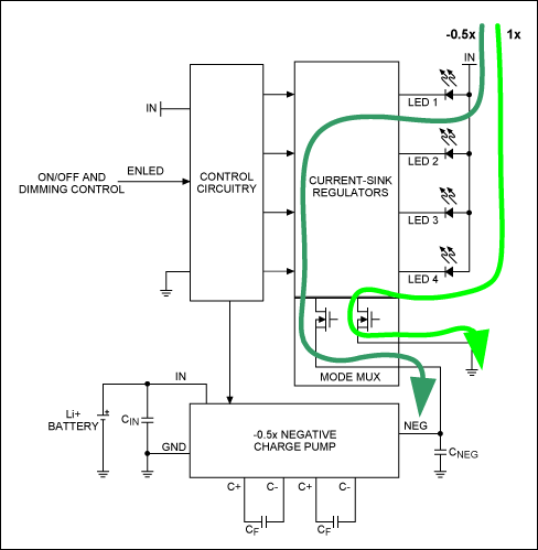
Figure 2. Each WLED can be switched individually when the driver is switched to negative charge pump mode, improving overall efficiency.
Improve the efficiency of any LED forward voltage. For traditional 1 × / 1.5 × positive charge pump WLED driver, the anode of WLED is connected to the output of the charge pump. If the WLED does not match, when the voltage margin (VIN-VLED) cannot meet the worst-case WLED forward voltage, the driver must switch to 1.5 times the voltage mode.
For the negative charge pump structure, there is no need to abandon the efficient 1x voltage mode because the forward voltage of only one WLED does not meet the requirements. As shown in FIG. 2, the mode multiplexing circuit individually selects 1x voltage mode or -0.5 for each WLED Double voltage mode to maximize the overall efficiency.
For example, when the input voltage is not high enough to meet the WLED maximum forward voltage requirement, the MAX8647 / MAX8648 charge pump driver turns on -0.5 times the charge pump. In this case, the device only drives the WLED with the highest VF through -0.5 times the negative power supply (instead of ground), while other WLEDs with lower forward voltages are still in the 1x voltage mode.
To further improve efficiency, the MAX8647 / MAX8648 provide independent mode conversion for each WLED. The technology can adaptively switch WLED to -0.5 times the voltage mode at different times and under different VIN conditions according to VF mismatch or temperature changes (Figure 3).
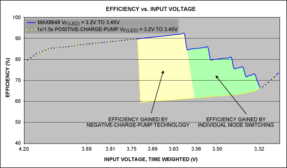
Figure 3. When the MAX8647 / MAX8648 charge pump WLED driver is switched to negative charge pump mode, each WLED can be individually switched to improve efficiency.
Summary In traditional schemes, WLED backlight designs using charge pumps are often less efficient than inductor-based designs. When the current of any WLED is lower than the predetermined level, the positive charge pump structure will switch the mode and no longer work in the most efficient 1x voltage mode. Therefore, when the system uses a large number of WLEDs and has a high forward voltage mismatch, a lot of power will be wasted.
The negative charge pump structure overcomes the shortcomings that the positive charge pump design usually has inefficient. Devices such as the MAX8647 / MAX8648 use a negative charge pump structure, and can switch modes individually for each LED, which can significantly improve efficiency and extend battery operating time. These WLED drivers provide designers with the same efficiency as inductive circuits, while still maintaining the simplicity and low cost of charge pump solutions.
Face Mask play a very important protective
role in the outbreak, mainly to protect the respiratory tract, can prevent the
spread of respiratory droplets, reduce the invasion of viruses or bacteria,
prevent the role of infection, but also can prevent the invasion of harmful
substances, also can reduce the probability of cross-infection.
In the outbreak to correctly choose masks and use Medical Masks,
Disposable mask, to choose the application of surgical masks or n95 masks, such
as disposable cotton masks, disposable paper masks, and anti-smog masks are not
recommended to wear, because their tightness is not good, cannot prevent
viruses and bacteria, play a preventive role.
At the same time, wearing a mask cannot be used continuously
for a long time, it is generally recommended to change every four hours,
wearing for a long time may absorb more viruses or bacteria on the surface of
the mask and reduce the defense ability.
Face Mask
N95 mask,Medical masks,Disposable mask,Protective mask
YFJ TECHNOLOGY (HK) CO.,LIMITED , http://www.yfjpower.com