In recent years, the global energy crisis has intensified, and conventional energy sources have been unable to meet the needs of world economic development. As an important renewable green energy source, solar energy has been favored by countries all over the world. The solar semiconductor lighting system integrates the advantages of semiconductor and solar energy resources, effectively improving lighting efficiency and green energy saving. In practical applications, it should increase the analysis and research of solar semiconductor lighting systems, and give full play to the advantages of solar semiconductor lighting systems.
Overview of solar semiconductor device characteristics
The solar semiconductor is mainly composed of an optical system, an electrode, a PN junction chip, etc., and the illuminant area of ​​the wafer is about 0.025 square millimeter. The whole illuminating process goes through three stages: injecting carriers under forward bias conditions; optical energy transmission; composite radiation . A semiconductor wafer is encapsulated in an epoxy resin. When electrons flow through the wafer, positively charged electrons and negatively charged electrons recombine in the hole region, and holes and electrons disappear to generate photons, photon energy and holes, and electrons. The band gap is proportional, and the light color corresponds to the photon energy. According to the visible light spectrum analysis, the red light and the orange light have the least light energy, and the purple light and the blue light have the most light energy.
With the rapid development of packaging technology and material technology, the green LED light efficiency is about 50lm/W, and the orange and red LED light efficiency is 100lm/W. The full color, high brightness and high efficiency of LED are more and more applicable. Widely used, especially in outdoor lighting systems. LEDs achieve all the visible light in terms of chromaticity, especially the emergence of ultra-high brightness white LEDs, which promotes the rapid development of illumination sources.
In general, light intensity 1cd is the boundary between high-brightness LED and ordinary LED. GalnAs, AILnGaP and A1GaAs materials are mainly used to process high-brightness LEDs. High-brightness red LEDs use A1GaAs material, high-brightness yellow-green, yellow, orange. The red LED uses AILnGaP, and the high-brightness violet, blue and dark green LEDs use GalnAs.
The luminous efficiency of LED semiconductors is high. The luminous efficacy of tungsten halogen lamps and incandescent lamps is 12~20 lumens/watt, high-pressure sodium is 90~130 lumens/watt, fluorescent lamps are 50~60 lumens/watt, and the spectrum is narrow and the monochromaticity is good. It does not need to be filtered to emit colored visible light. At the same time, LED is an all-solid illuminant, which is resistant to shock and shock, and is not easily broken. It can be developed into a small and light lighting product, which is convenient for maintenance, repair and installation. Moreover, the startup time of the LED light source is short, and the characteristics of the gas discharge light source largely determine the startup time. The semiconductor light source encapsulated by epoxy does not contain components such as filaments, glass and the like which are easily damaged, and can pass through. Shock and vibration.
Solar semiconductor lighting system design
(1) System composition
The solar semiconductor lighting system consists of a semiconductor lighting load, a controller, a battery, and a solar cell. The standby power supply is set in the basic structural frame. Through the standby power supply, the semiconductor lighting load can be continuously supplied by the backup power source even if it is continuously raining for a long time. To ensure that the solar semiconductor lighting system can operate safely and stably when the battery cannot be powered in time.
When the solar semiconductor lighting system is in operation, solar radiation can be converted into electric energy through solar cells. The solar radiation intensity and temperature have a direct impact on the solar cell output power. When the radiation intensity is weak and the temperature is low, the battery output power cannot always be stable. Sexuality, therefore, it is necessary to store electrical energy in time through the battery during the period of high solar radiation intensity, so that it is convenient to supply power to the semiconductor lighting system reliably and stably during the operation of the lighting system.
The controller is the core of the solar semiconductor lighting system. The controller scientifically manages the battery charging and discharging process, effectively controls the working state of the lighting system, and enables the solar semiconductor lighting system to operate smoothly under different working conditions.
(2) Conversion process
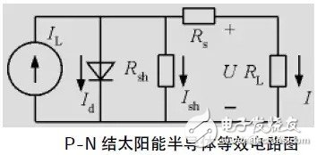
Semiconductor materials are important structural materials for solar cells. The most important characteristic is the photovoltaic effect, the equivalent circuit diagram of PN junction solar semiconductor. As shown in the figure, the semiconductor has a photovoltaic effect after receiving solar radiation, after the following three conversion stages.
1) Generate an electron pair. In the absolute zero state, the semiconductor forms a dielectric band inside, and the conduction band does not contain electrons. Under normal conditions, the semiconductor can be regarded as an insulator and does not exhibit conductivity. When solar energy is radiated to the semiconductor, the forbidden band width is much smaller than the photon energy, and the semiconductor absorbs the light quickly. If the semiconductor crystal lattice absorbs more of the solar radiation, it can be separated from the electron lattice of the semiconductor, resulting in a large amount of Free electrons form holes. Therefore, in order to convert the semiconductor lattice-constrained electrons into a large number of free electrons, the semiconductor band gap should be smaller than the photon energy, for example, the silicon forbidden band width is 1.15 ev, the semiconductor band gap and the incident light energy are kept consistent, and the light absorption efficiency is Higher, a large number of hole-electron pairs can be generated. However, when a photon with a larger energy is injected into the semiconductor, a part of the photons are absorbed by the semiconductor lattice, and a part of the energy is lost, resulting in a decrease in luminous efficiency;
2) Hole-electron pair separation. When there is no electric field around the solar semiconductor illumination system, a large number of photoexcited hole-electron pairs are uniformly distributed in the semiconductor. Since no current flows through the external circuit, it is necessary to use some way to generate a potential barrier in the solar semiconductor to ensure excitation. The hole-to-electron pair is separated and continuously supplies power to the circuitry outside the lighting system. Normally, the PN junction is mainly used to achieve this barrier. The effect of the PN junction on hole-electron separation is limited. If no external circuit is provided, the separated electrons are concentrated in the P and N layers, PN. The junction is positive and gradually deflects toward the direction in which the potential barrier is lowered. After the separation stops, it returns to the normal state. The voltage between the PN junctions is called the open circuit voltage, and the amount of illumination light is proportional to the short circuit current;
3) Carrier movement. The hole-electron pair is not necessarily completely separated under the condition of light energy radiation, and the ratio of the number of separations to the number of generations is called collection efficiency, and moves under the effects of charge concentration gradient and electric field shift effect. Normally, carriers have a tendency to automatically restore equilibrium. If the excess carrier lifetime is shorter than the PN junction electron mobility time, the PN junction position and excess carrier lifetime have a decisive influence on the collection efficiency, and the holes move to P. In the layer, the electron moves to the N layer, and the positive and negative charges are respectively concentrated on the semiconductor beam, and the ends are connected by wires to generate an electric current.
Conclusion
In recent years, solar semiconductor lighting systems have developed rapidly and are widely used in various lighting fields. Combined with the application characteristics of solar semiconductor devices, the semiconductor lighting system will be further optimized and improved in the future development process, and its luminous efficiency will be continuously improved.
Circular Emergency Ceiling Light is according to the type can be divided into maintenance or non-maintenance . It is made of solid polycarbonate material , with protection rating of IP65 , suitable for indoor and outdoor use . It comes with a premium rechargeable lithium-ion battery with automatic monthly and annual detection .

Emergency Ceiling Light
Emergency Light Ceiling,Industrial Emergency Light,Led Emergency Ceiling Lights,Ceiling Mounted Emergency Lights
Jiangmen City Pengjiang District Qihui Lighting Electrical Appliances Co., Ltd , https://www.qihuilights.com