Abstract: The wireless sensor network data acquisition system is designed with C8051F020 as the core processor. The system adopts SZ05-ADV wireless communication module to build Zigbee wireless network, combined with the hardware and software technology of embedded system, completes the data acquisition of 8 sensor signals of terminal nodes. After the 8-channel signal is processed by the front-end, it is sent to the C8051F020 12-bit A/D converter for conversion. Field data that has been accurately processed and stored. Through the Zigbee wireless network to the host computer, the system can achieve the purpose of wireless testing in automotive testing.
Keywords: Zigbee; wireless network; C8051F020; embedded system
This article refers to the address: http://
Automobile testing is an important means to discover various problems in the design and development of automobiles. Based on the test results, it can make an objective evaluation of various performances of automobiles. As one of the basic projects of the automotive industry, automotive testing has played an important role in the overall development of the automotive industry. The automotive performance test system is a key component of the automotive test project. It is composed of several interconnected and interacting sensors and instruments. It is an organic whole composed of tests for the performance of the car. The performance of the automotive test system. It often has a major impact on the effectiveness of the entire vehicle test. The existing automotive test systems mostly use wired connections. There are two drawbacks in this way: 1) The automotive test needs to be carried out in a harsh environment such as a large dedicated test site or a typical area. The field wiring task is cumbersome and error-prone; 2) some automotive tests If the serpentine test is highly dangerous, it is more important for test systems that can reduce test losses. The system uses Cygnal's C8051F020 microcontroller as the control core. Based on Zigbee wireless network technology design, for example, multi-channel data integrated acquisition system, it uses fewer peripheral devices to test the performance parameters in the automotive test, shortening the field wiring time and improving the time. Test efficiency and reduce accident losses when test accidents occur.
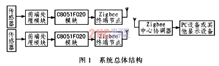
1 System overall structural design The automotive test mainly includes test items such as power performance, fuel economy, steering stability and emission characteristics. The main performance parameters include speed, acceleration, fuel consumption, temperature and dynamic motion parameters in the steering stability test. The test signals of these parameters obtained by the sensor are processed into the C805l-F020 microprocessor after being processed (shaping, filtering, amplifying, etc.) by the front-end processing module, and the analog-to-digital conversion and data processing are performed inside the single-chip microcomputer through the serial port. The Zigbee terminal node is connected, and then the terminal node sends data in the WLAN. After receiving the data, the Zi-gbee central node communicates with the host computer through the serial port. The central node can also send the command of the upper computer to the terminal node to control the terminal node to execute. The overall structure of the system is shown in Figure 1.
2 system hardware design
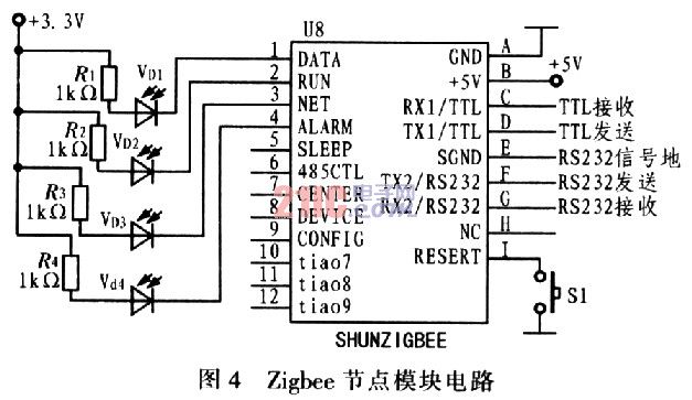
2.1 Front-end processing module The sensor converts various common non-electrical signals into power signals, which are generally weak. The front-end processing module processes these signals and sends them to the A/D conversion port of the microcontroller. The system has a total of 8 sensor signals, including 2 voltage-variable sensor signals, 2 -5 ~ +5 V voltage signals, 2 4 ~ 20 mA current signals and 2 front-end processing of thermocouple signals. The front-end processing hardware circuits of the pressure-variable sensor signal and the thermocouple signal are shown in FIG. 2 and FIG. 3, respectively.
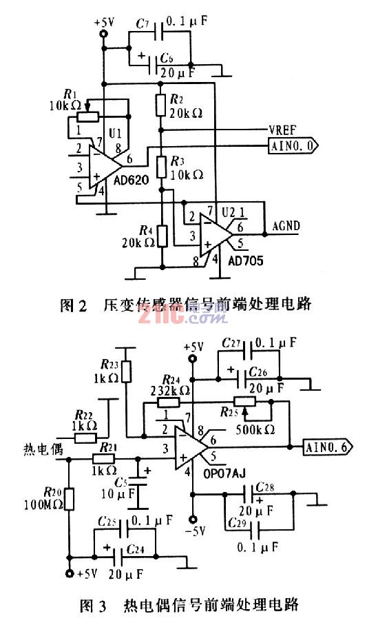
The AD620 is a low-cost, high-precision instrumentation amplifier that requires only one external resistor to set the gain with a gain range of 1 to 10,000. The front-end processing of the pressure-variable sensor signal uses an amplifier circuit composed of AD62-0 and AD705. This part is powered by a single power supply. The AD705 is a voltage follower that provides the zero point of the output voltage for the AD620. Send VREF, AGND to the AINl of the 8-bit precision AD-Cl of the MCU. 0, AINl. 1 port, using the software program to achieve the reference voltage of the road signal and the calculation of the analog ground.
The thermocouple sensor is used to measure the temperature of key components of the car. The front-end processing circuit uses the adjustable gain amplifier circuit of OP07. OP07 is a low noise, non-chopper-stabilized bipolar op amp IC with very low input offset voltage. Low offset and high open loop gain make OP07 especially suitable for high gain measurement equipment and amplification sensors. Weak signal, etc. In the case where the accuracy is not high, the offset voltage of OP07 can be neglected. In this circuit, R25 and R24 are used to adjust the system amplification factor. When different types of thermocouples are selected, the resistance values ​​of the two can be adjusted appropriately.
2.2 C8051F020 Module C805lF020 is a mixed-signal SOC 8-bit microcontroller from Cygnal Corporation. It is a fully integrated mixed-signal system-level MCU device with 64 digital I/O pins. The microcontroller uses a high-speed 805l microcontroller core with a speed of up to 25 MI/s, 8 I/O ports, 5 general-purpose timers, 5 capture/compare modules and a dedicated watchdog timer. -Bus, SPI and 2 UART serial ports with built-in 64 kB high speed memory. For analog peripherals, the device features a 12-bit A/D converter, an 8-bit A/D converter, two 12-bit D/A converters, and two analog comparators. These digital and analog peripherals within the device make the design of the system simpler and more integrated.
This module mainly designs the reset circuit of C8051F020, external crystal oscillator circuit and grounding processing, and leads all the pins out to expand the application. The system needs high-speed operation to collect data in a timely and efficient manner. Therefore, the microcontroller uses the internal oscillator as the clock source under normal circumstances. However, due to the large error of the internal clock, in the process of serial communication, an external clock should be selected, and the internal and external clocks can be switched through software settings. By connecting the decoupling capacitor to the analog ground at the power supply, the area of ​​the interference loop can be reduced, the electromagnetic interference radiation can be reduced, and the interference caused by the digital current can be coupled to the ground without appearing in the ground of the external circuit. In order to minimize the capacitive coupling, the two do not overlap, and the two independent grounds are connected together by ceramic beads at the common "star" type of the power source, and similar processing is applied at the power source to prevent interference.
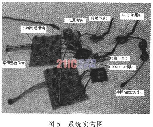
2.3 Zigbee node module The automotive test system studied in this paper initially adopts two terminal nodes and one central coordinator to form the topology of the star network. All three nodes use SZ05-ADV wireless transceiver module, Zig-bee terminal node. The central node and the C8051F020 module and the PC device are respectively connected through the standard serial port to realize wireless transmission of data. The SZ05-ADV is a high-performance embedded wireless transceiver module. Its core device is Freescale's MCl3213. It is the second-generation standard ZigBee wireless communication platform that integrates a low-power 2.4 GHz RF transceiver and 8-bit microcontroller in a 9 mmx9 mmxl mm 7l-pin LGA package with 60 kB of flash memory for the MCl3213 device. The MCl32lx solution can be used as a wireless connection in a simple point-to-point connection to a complete ZigBee mesh network. The combination of a radio transceiver and a microcontroller in a small footprint package makes it a cost-effective solution in the MCl321x. The RF transceiver operates in the 2.4 GHz ISM band and is compatible with the 802.15.4 standard. The transceiver includes a low noise amplifier, 1 mW of RF output power, a power amplifier (PA) with VCO, and an integrated transmit/receive switch. The on-board power regulator and full spread spectrum encoding and decoding, the microcontroller in the MCl32lx is based on the HCS08 family of microcontroller units (MCUs), HCS08 A version, up to 60 kB of flash and 4 kB of RAM.
The SZ05-ADV embedded wireless communication module integrates the RF transceiver and microprocessor complying with the ZIGBEE protocol standard. The data interface includes: TTL level transceiver interface and standard serial port RS2-32 data interface, which can realize data transmission and transmission. Destination address transmission mode. In addition to the general point-to-point data communication function, data communication between multiple points can be realized. Its module connection circuit is shown as in Fig. 4. DATA, RUN, NET, and ALARM are the four working status indication ports of the SZ05-ADV wireless communication module, which are data transmission and reception, system operation, network status and alarm. The SLEEP pin is used to control the system into a low-power state, low-level into low-power, high-level or floating normally.
The 485CTL pin is a 485 transceiver control. The module 485 receives a low level output and transmits a high level output. The CENTER and DEVICE pins are node function configuration interfaces, all of which are active low, or connected to the pin tiao7 and tiao8 respectively. If the two pins are high or floating, they are routing nodes. The CONFIG pin is a configuration interface, active low, or a jumper cap that allows you to enter the system configuration state in the HyperTerminal. The standard operating voltage of the module is DC-5V, and the normal working voltage range is 5~12V. The data interface has two interface modes: RS-232 and TTL. The RS-232 serial port is the three-wire working mode of TX2, RX2 and SGND. The TTL is the two-wire working mode of TX1 and RXl, and the TTL level is 3.3V. RESET enters the low state for 3s, the system enters the configuration state, and the high level or floating state enters the working state.
The wireless communication network node can be divided into a central coordinator, a router and a terminal node according to functions. The central coordinator is the central node of the network, responsible for the initiation organization, network maintenance and management functions of the network; the router is responsible for routing and forwarding of data, and the terminal node Only the data of this node is sent. In the system, the wireless module can be configured in advance in the computer super terminal, such as the node type, the node name and the address, the radio frequency point, the network ID, the baud rate, and the data type. The internet.
3 Software Design System program development uses the special integrated development environment of the C805lF series MCU Silicon Laboratories IDE, configured with Keil C5l assembler, linker and compiler. The use of C5l development programs facilitates the modularization of system programs and increases their portability, and can reduce the development cycle. The system software consists of three subroutines: main program and A/D conversion, data processing and communication. The main program part includes subroutine such as system initialization, calling A/D conversion, data processing, and serial port transmission. The initialization part includes: initial setting of watchdog module, setting of system clock and reset source, initialization of I/O port, initialization of serial communication interface, initialization of A/D conversion, and timer initialization. The maximum conversion speed of ADC0 is . 100 ks/-s, whose conversion clock is derived from the system clock division, and the division value is held in the ADCSC bit of the ADCOCF register. In the system on chip, 8 channels need to be acquired, and the sampling frequency is set to 50 000 times/s. The selected ADCO conversion start mode is Timer 3 overflow (ie, timing continuous conversion) mode.
4 Test After programming the program into the C805117020 through the U-EC2 dedicated programmer in the Silicon Laboratories IDE, connect the modules for debugging, as shown in Figure 5. 8 channels of sensor signals (including 2 voltage-variable sensors, 2 channels -5 to +5 V signals, 2 channels of 4 to 20 mA signals and 2 channels of thermocouple signals) are processed by the front end and sent to the MCU via A/D conversion and After the data is processed, it is output to the Zigbee terminal node through the serial port and sent in the wireless network according to the destination address mode or the broadcast mode. The Zigbee central coordinator and the host computer are connected through the standard RS232 serial port, and can be viewed in the HyperTerminal or the serial port debugger. data. This research focuses on experimental development. The power module can use the common 220 V to double 9 V transformer. After the rectifier bridge, the LM7805 and LM7905 are regulated to output -5 V and +5 V (3.3 V voltage can be used.) After the AMSlll7 module is converted, a dedicated power module can be designed for practical use. The test results show that the system can realize the data sampling of the 8 sensors of the two terminal nodes. The Zigbee wireless network runs normally, and the real-time data of the test can be seen in the HyperTerminal.
5 Conclusion The vehicle test system based on C805lF020 and Zigbee wireless network designed in this paper realizes the wireless transmission of data in the automobile test, which simplifies the test site wiring and improves the test efficiency. Once the test accident occurs, the loss is greatly reduced. The experiment proves The system replaces the feasibility of a traditional automotive test system, and the system is also easier to expand, enabling more functions. This research focuses on the application development of Zigbee wireless network, which can provide some reference for the application of Zigbee technology in sensor networks, but it is limited to the software program system and the experimental electromagnetic interference. The synchronization mechanism and anti-interference performance of the system need further the study.
In Ear Bluetooth Headphones with Perfect
HIFI Quality Adopt Bluetooth CSR 4.2 technology, built-in CVC 6.0 Noise
Cancelling technology, and professional sound chamber design, from the phone to
earphones, from the Bluetooth Headphones to ears, or internal circuitry, every stage is
always designed for perfect sound experience.
This Bluetooth Headphone brings no burden to your ear and make you
feel comfortable long time! It is very simple and easy to operate with one hand
to realize multi-functions by just touching the earbuds, such as music play /
pause, call start / end / rejection / redial . Also you can modulate the volume
by touching it twice (turn up)or three times(turn down)! How miraculous it is!
In Ear Bluetooth Headphones,In-Ear Wireless Bluetooth,Wireless In Ear Headphones,In-Ear Wireless Earbuds
ShenDaDian(China) Digital Electronics Co.,Ltd , http://www.btearbuds.com