Xilinx IP core configuration, step by step to verify Xilinx Serdes GTX up to 8.0Gbps
Before using SerDes, I was working on relatively low-speed applications at 3.125 Gbps. Following the official documentation step by step, everything worked smoothly. However, this time I wanted to test the maximum line speed of the K7 series GTX, which is up to 8 Gbps, and see if it aligns with what the Xilinx documentation says.
How fast can the GTX run? To find out, I referred to the official data sheet for the Kintex-7 FPGA, specifically DS182: DC and AC Switching Characteristics. This document provides critical information about the device’s performance, including maximum frequency, setup and hold times, and other timing parameters that are essential for high-speed design. These details help in selecting the right part for your application, especially when designing for higher speeds.
Next, I looked into the GTX Transceiver Switching Characteristics. As per the data sheet, the K7 series GTX can support up to 12.5 Gbps, but this depends on the speed grade and package type. For instance, the -3 speed grade with an FF package allows for the highest speed of 12.5 Gbps. However, the chip I’m working with is a K7480TFFG901-1, which only supports up to 8 Gbps. This is also confirmed during IP core configuration, where the line speed range is listed as (0.5–8.0). So, the IP core is closely tied to the specific device, and Vivado has made this process much more user-friendly over time.
Step-by-step IP Core Configuration
The following steps are based on my experience and can be helpful for beginners. When setting up the IP core for the first time, you might feel overwhelmed by the number of files generated and the numerous IO ports. But once you get the hang of it, it becomes routine.
1. First, search for "GT" in the IP catalog and select the 7 Series FPGAs Transceivers Wizard.
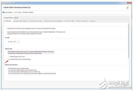
I gave it a name and chose to include shared logic in the example design. I had encountered some issues before when certain resources needed to be shared, like with an Ethernet RGMII module. In such cases, it's important to use IODELAY_CTRL and ensure that the same IOB isn't used elsewhere. It's safer to go with the second option to avoid conflicts.
2. Next, the most important part: setting up the transceiver parameters.
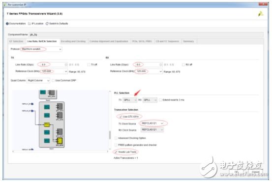
I selected the protocol from scratch without any agreement. Then I set the line speed to 8 Gbps, within the allowed range (0.5–8.0). The reference clock was chosen based on the software’s recommendations. The receiver settings were also configured, and since it's full-duplex, I could choose to disable either the transmitter or receiver if needed. PLL selection was based on the data sheet, and I found that the line speed had already determined the available options.
Choosing the right transceiver is crucial and depends on the design. I referenced the schematic to determine which transceiver to use.
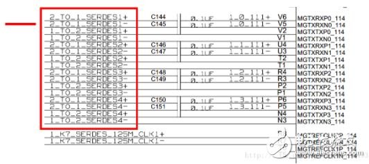
According to the manual UG476, I checked the placement information for the package and found that X0Y8 was being used. The input clock was located in the same group as clk0. Finally, I used Vivado Lab Tools to generate the example project for reference.
3. Continuing the configuration, I decided to use 64b66b encoding instead of 8b10b. 64b66b is more efficient and is commonly used in high-bandwidth applications. The reason for choosing one over the other lies in the scrambling code, which helps improve CDR performance and reduce DC components.
4. The optional ports were simplified by removing unnecessary ones.
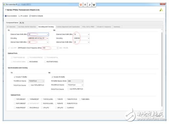
Since there was no option for 8b10b, the page was not configurable, and all optional ports below were removed.
5. PCIe was kept for future study, as it's more complex. Optional ports, however, are useful for adding control features, such as loopback. There are four internal loopback modes: normal, near-end PCS, near-end PMA, and remote PMA/PCS.
6. Channel bonding and clock correction were also configured. Channel bonding aligns multiple physical channels into a single logical channel, using FIFO to manage delay differences. Since we’re only using one channel, binding wasn’t necessary.
7. Finally, I verified the transceiver clock. The clock was set to 250 MHz, which makes sense because 8 Gbps divided by 32 equals 250 MHz.

At this point, I had completed more than half of the configuration.
Generating the Example Project
After configuring the IP, I generated the example project. I then modified the XDC constraint file to assign the input clock to the appropriate pin.
## LOC constraints for DRP_CLK_P/N
Set_property LOC G27 [get_ports DRP_CLK_IN_P]
Set_property LOC F27 [get_ports DRP_CLK_IN_N]
Set_property IOSTANDARD LVDS_25 [get_ports DRP_CLK_IN_P]
Set_property IOSTANDARD LVDS_25 [get_ports DRP_CLK_IN_N]
I also constrained the GTX transceiver location and adjusted the clock pins accordingly. Additionally, I modified the ILA core to monitor the data after descrambling, making it easier to observe the received data.
Board Debugging and Verification
Once the bitstream was generated, I connected the FPGA via a serdes link or set up internal loopback for testing. Using two FPGAs for cross-testing also proved effective.
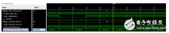
The error count remained zero, confirming that the transceiver was functioning correctly. The received data matched the transmitted data, showing that the system was stable and reliable.
The experiment confirmed that the GTX can indeed operate at 8 Gbps. The example project includes scrambling and descrambling logic, allowing for detailed analysis of the data. You can modify the output after descrambling to compare it with the original data and observe how the verification module works. This is a great learning opportunity for anyone working with high-speed serial communication.
CZUR book scanner,book page scanner,handheld book scanner,book to pdf scanner
Guangdong ZhiPing Touch Technology Co., Ltd. , https://www.zhipingtouch.com