Question: Can I use the disable pin of the amplifier to save power without affecting performance?
Question: Can I use the disable pin of the amplifier to save power without affecting performance?
In today’s Internet of Things (IoT) era, battery-powered devices are becoming more and more common. This article explains how you can optimize both power efficiency and signal accuracy without compromise.
Many operational amplifiers come with a disable pin that, when used correctly, can reduce power consumption by up to 99% without compromising signal integrity. The disable pin is typically used for static operation or standby mode. In this state, the IC enters a low-power mode and doesn’t need to process any signals, significantly reducing power usage.
If the op amp is used as a buffer for an ADC, as shown in Figure 1, it needs to be active to perform its function. However, if the disable pin is activated, the device can enter shutdown mode, maintaining low power consumption. This is especially useful when the ADC isn't sampling new data.
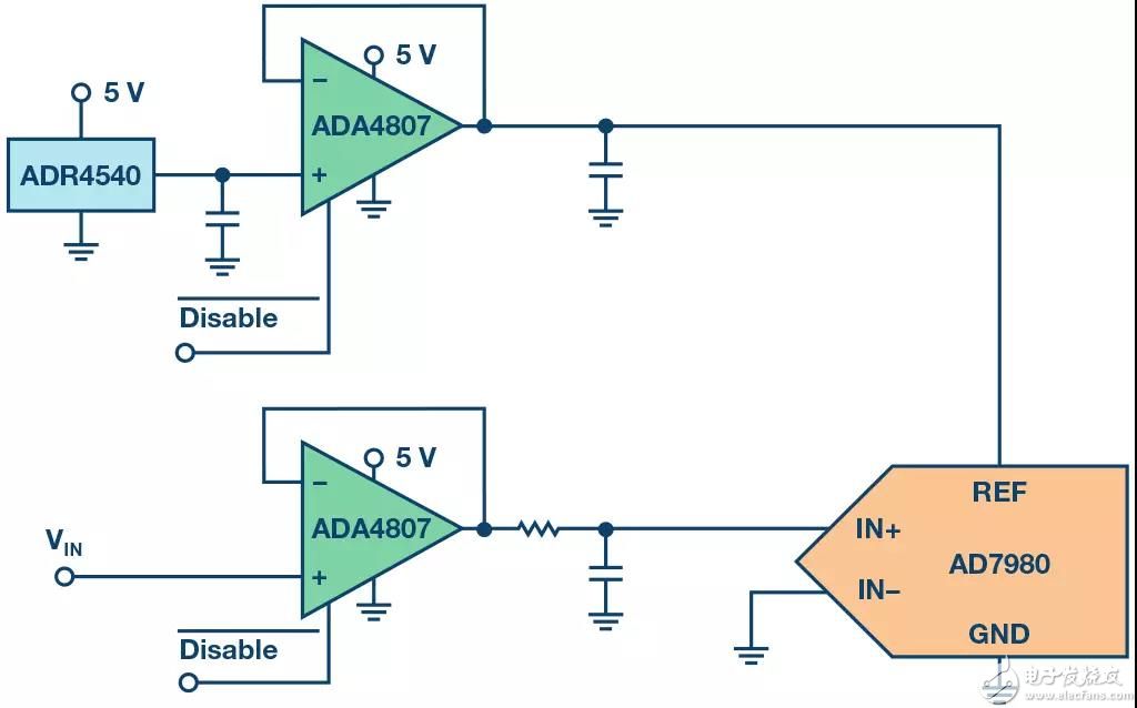
Figure 1. Typical schematic of an ADC input stage with ADC driver and reference buffer.
One effective way to implement this is by using the ADC’s start command. During a standard ADC conversion, the input capacitor is first charged to the voltage being measured before the conversion begins. Once the capacitor is isolated, the conversion starts. The duration of this process depends on the ADC type and configuration.
So, the key question is: When must the op amp be active? It needs to operate long enough before the conversion starts to ensure the internal input capacitor reaches the correct voltage. The required time depends on the capacitor size, the voltage level, and the amplifier’s ability to drive capacitive loads.
The AD7980 ADC datasheet specifies a 400Ω impedance with 30 pF of input capacitance. But op amps are not so simple. While the parameter table may list a 15 pF capacitive load, real-world scenarios can involve higher values. For example, a low-pass filter with 2.7 nF and 20 Ω could add to the total load.
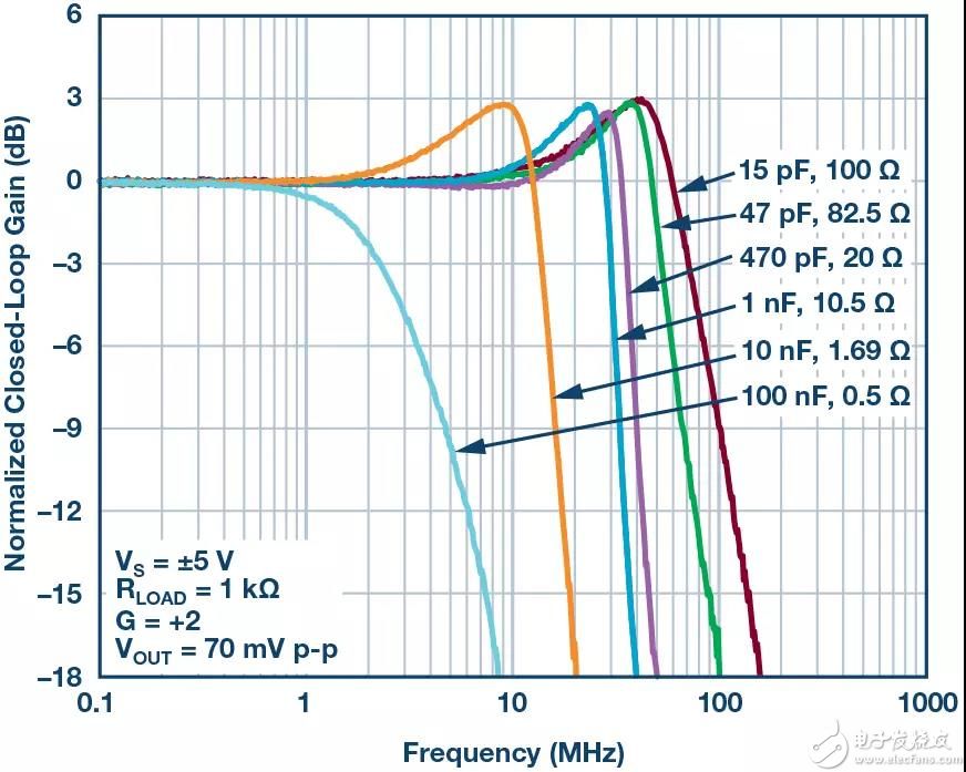
Figure 2. Frequency response of the ADA4807.
As shown in this graph, the amplifier can handle high capacitive loads effectively. When disabled, it takes about 500 ns to reach full-scale output, which is either 5 V or 4.096 V depending on the application.
To be safe, we assume the amplifier turns on 750 ns before the conversion starts. At 1 kSPS, this results in a power saving of 99.83% (only 0.02 mW consumed). At 1 MSPS, the savings drop to 92.41%, but still result in only 10.75 mW total consumption. This is just the power saved by the ADC driver — the reference buffer also benefits from the same technique.
This example demonstrates the capabilities of modern components. With a minimum sampling time of 500 ns, the SINAD deviation remains below 0.5 dB. For drivers, it's important to consider faster devices and apply them appropriately. We've only looked at a buffer configuration (gain = 1), but for inverting or other configurations, power savings will vary. These cases should be verified through testing and measurement.
Telephone Cable
Standard: AS/ACIF S008 and ISO/IEC 11801, AS/NZS 3080
Conductor: Plain annealed copper
Insulation: Solid polyethylene
Tape: Polyester Tape
Sheath: PVC (Polyvinyl Chloride)
Applications: Those Communication Cable is designed for use within telephone exchanges, commercial switchboards and interconnecting wiring systems
Telephone Cable, phone cable,signal cable
Shenzhen Bendakang Cables Holding Co., Ltd , https://www.bdkcables.com