Researchers at the University of Wisconsin-Madison (UW-Madison) claim to create the fastest and extensible wearable integrated circuit (IC), a development that is expected to drive the Internet of Things (IoT) and More connected high-speed wireless world progress.
Engineers have created a platform for manufacturers looking to expand the capabilities and applications of wearable electronics, especially those that are leveraging next-generation wireless broadband technologies (ie 5G).
This extensible circuit has a unique structure, primarily due to the twisted pair of telephone lines. Basically, it contains two ultra-slim interleaved power transmission lines in a repeating S-curve mode.
This layered winding shape – consisting of two layers of segmented metal blocks, like a 3D puzzle – gives the transmission line the ability to stretch without compromising performance. It also helps protect these lines from outside interference while limiting the electromagnetic waves flowing through them, virtually eliminating current losses. Currently, these scalable integrated circuits can operate at up to 40 GHz frequency modulation (RF).
In addition, these new extensible circuits are only 25 microns (or 0.025 mm) thick compared to other extendable transmission lines that may reach 640 microns (or 0.64 mm) in width. This is extremely small and even small enough to achieve high efficiency in a variety of applications such as skin electronics.
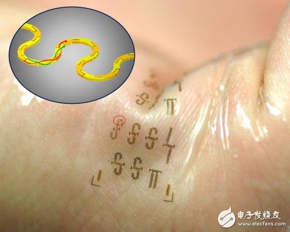
This new circuit uses a 3D puzzle-like interlocking manufacturing method that can be used for wearable electronics attached to the skin like a tattoo sticker. Because such circuits increase the speed of wireless, these systems allow healthcare professionals to remotely monitor patients without having to use any wires or cables.
Source:Yei Hwan Jung and Juhwan Lee/UW-Madison
The research team led by Zhenqiang (Jack) Ma, a professor of electronics and computer engineering at UW-Madison, published this powerful and efficient IC research detail in the journal Advanced FuncTIonal Materials.
Over the past decade, Ma's research team has been working on the development of so-called active transistor components. This latest development combines the expertise of researchers in the field of high frequency and soft electronics.
The study was supported by the Air Force Office of ScienTIfic Research. “We have found a new way to integrate high-frequency active transistors into efficient circuits that can be transmitted wirelessly,†Ma said. “This is a platform that opens the door to many new features.†In mobile communications, the wide microwave radio frequency of 5G networks will be able to accommodate more and more mobile phone users, while significantly increasing data rates and coverage.
In the intensive care unit, the epidermal electronic system (electronics attached to the skin like a tattoo sticker) allows medical personnel to remotely monitor the patient wirelessly, improving patient comfort by reducing the entanglement of cables and wires.
Other authors of this article include UW-Madison's Yei Hwan Jung, Juhwan Lee, Namki Cho, Sang June Cho, Huilong Zhang, Subin Lee, Tong June Kim and Shaoqin Gong, and the University of Electronic Science and Technology. Yijie Qiu of Technology of China and others.
Compile: Susan Hong
Double-sided PCBs are one of the most common kinds available. While single-sided PCBs have one conductive surface, double-sided PCBs have a conductive layer on each side. A dielectric layer is surrounded by circuit copper layers and solder mask on both sides. Vias allow manufacturers to create traces on both sides that route around each other and connect between layers. Manufacturers use double-sided PCBs for products that need a beginner to intermediate level of circuit complexity. This type of PCB doesn`t offer as much circuit complexity or density as multilayer PCBs, but they work as an affordable option in numerous applications
Double-Sided PCB, Double-Sided PCB With Enig Via In Pad PCB, FR4 PCB With Matt Black Soldermask
Storm Circuit Technology Ltd , https://www.stormpcb.com