Cars have begun to enter the family of our country, and high-power car audio with superior performance is increasingly favored. In the past, car audio power was directly used for 12V lead storage batteries, so that the pulse and other interference generated by the car ignition directly became the main source of acoustic noise. The 12V low voltage single power supply also limits the audio output power, and the power amplifier circuit can only use the OTL circuit, and the frequency response characteristics are poor. With the development of components and advances in technology, switching power supplies have been fully applicable to car audio. It can provide dual power supply with high voltage, and can suppress the intrusion of various noises. The power amplifier circuit also adopts OCL circuit, which makes the car audio effect truly grade. The switching power supply for car audio application meets the needs of technological development.
This article refers to the address: http://
Figure 1 is a car audio switching power supply circuit, the circuit is mainly composed of two integrated circuits TL494 and KIA358, drive tubes Q702 and Q703, switch tubes M704 ~ M709, transformers, output rectifiers and filters. The TL494 is a pulse width modulation switching power supply integrated controller with a maximum drive current of 250mA and an operating frequency of 1 to 300kHz. The output mode is either push-pull or single-ended. The internal block diagram is shown in Figure 2. For details, refer to the TL494 Pulse Width Modulation Control Circuit. It mainly consists of a triangular wave oscillator, two comparators CMP1 and CMP2, two error amplifiers A1 and A2, a 5V reference voltage source, a flip-flop and an output driver.
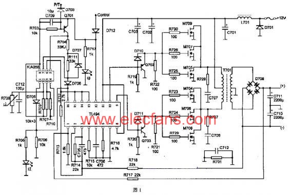
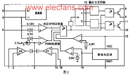
The triangular wave oscillation frequency is determined by external Ct and Rt of pins 5 and 6. The oscillation frequency is fosc=1.2/Rt×Ct. The triangular wave oscillation signal is sent to the two comparators, that is, the dead time comparator and the PWM comparator. The two comparators output to or Door circuit. Thus, the OR gate output level is inverted only when the amplitude of the oscillating signal level is higher than the dead time control level and the error input level. The pulse output is controlled by the trigger and the 13-pin output mode. When the 13-pin is connected to the low level, the internal trigger is disabled. The 13-pin of this circuit is connected to the high level (the reference voltage is 5V provided by the 14-pin), and the output two pulses are controlled by the flip-flops Q and Q respectively, and the maximum output pulse duty ratio is controlled by the two NOR gates and the push tube push-pull output. 48%, the frequency is half of the triangular wave oscillation frequency. The dead time is set by the voltage of 4 feet, and the range is between 0 and 3.3V. The error amplifier A1 is amplified as an output voltage sampling error, and as a result, the PWM comparator controls the pulse width to stabilize the output voltage. Error amplifier A2 is used for protection control. Pin 15 is connected to the reference voltage of 5V (provided by pin 14) and pin 16 is the control input. In the case of power-on protection, over-temperature or over-current protection, pin 16 is high. At this time, error amplifier A2 outputs a high level, which is higher than the amplitude of the oscillator triangle wave level, so that the driver has no drive pulse output. , the load is safely powered off.
The safety protection circuit is implemented by the KIA358 circuit. Provides a high level to pin 16 of the TL494 in the event of an abnormal condition. The KIA358 is a dual op amp circuit (Figure 3).

The op amp A1 is used for overcurrent protection, and the 6 pin is supplied with a 5V reference voltage from pin 14 of the TL494. Under normal circumstances, the P/T terminal is high level, and the 5 pin is low level. Therefore, the 7 pin output is low level, and the 16 pin of the TL494 is also low level. When the P/T terminal detects a low level due to an overcurrent or other cause of the op amp, the 5 pin is high level, and is higher than the 6 pin reference level, and the 7 pin outputs a high level to protect the action. The operational amplifier A2 is used for power-on protection and over-temperature protection. The voltage at the non-inverting input terminal is obtained by dividing the control voltage by 12V through two resistors R707 and R709. The inverting input voltage is obtained by dividing the voltage between R710 and thermistor R708. R708 has a resistance value of about 100kΩ at room temperature, a level of 2 feet is higher than the level of 3 feet, and a pin outputs a low level. When the temperature rises to nearly 100 ° C, the thermistor resistance drops below 10 kΩ. The level of 2 feet is lower than the level of 3 feet, the output is flipped, the protection action is activated, and the red LED is bright. Capacitor C712 is used for power-on protection. When the power is turned on, C712 is charged, and the level of 2 feet is lower than the level of 3 feet. At this time, the protection action and the red LED are bright. When the C712 is fully charged, the 2 pin level is higher than the 3 pin level, the 1 pin is flipped to the low level, the red LED is extinguished, the protection is cancelled, the operation is normal, and only the green LED is lit. The 14-pin reference voltage of the TL494 is provided by the 12-pin. The 12-pin is connected to the car power lock via the diode D712. Only when the car is turned on, the 12-pin has the working voltage, and the power supply works normally. The 9-pin and 10-pin outputs of the TL494 are buffered by Q703 and Q702 to drive the FET, and then boosted by the transformer, and after rectification and filtering, the sound is supplied to the sound in the form of a stable positive and negative power supply. Q702 and Q703 acting as switching transistors are connected without DC bias. When the 9-pin and 10-pin output drive signals of the TL494 are high, the signals are applied to the FET gate via diodes D711 and D710, respectively, when Q703 and Q702 are reverse biased. When the drive signal is low, Q703 and Q702 are turned on, and the charge accumulated in the gate capacitance of the FET is quickly discharged, causing the FET to turn off.
High frequency, high power, high efficiency, and specific requirements for car audio should be considered in component selection and circuit fabrication.
The switching power tube uses a metal oxide FET. Compared to a bipolar transistor, the power FET has many advantages:
1. The driving power is small, the driving circuit is simple, and the circuit structure is compact and miniaturized;
2. The cutoff frequency is high and no reverse bias is required;
3. Simple parallel connection can be implemented;
4. No secondary breakdown will occur;
5. There is no storage time;
6. There will be no thermal breakdown.
Since the battery supply voltage is only 12V, it is mainly considered to be able to withstand the current value of the conduction. When the power is large, the switch tube should adopt the multi-tube parallel connection. When the Vgs exceeds the turn-on threshold voltage, the ratio of the drain current to the gate voltage increases linearly. The rate of change of the drain current to the gate voltage, that is, the transconductance Gfs is actually a constant when the drain current is large. From Figure 4, the transconductance Gfs and drain current relationship diagram shows that the rise of the transconductance increases the gain of the MOSFET tube proportionally, which leads to an increase in the drain current, which in turn increases the input capacitance. Adding a push stage allows enough current to charge the input capacitor, reducing rise and fall times, and increasing the switching speed of the MOSFET. The push stage has a low enough output impedance to avoid positive feedback oscillations. In addition, the MOSFET is prone to oscillation when operating at high frequencies. Therefore, the length of the connection line to the MOSFET pin should be minimized during the board design, especially the length of the gate lead. Otherwise, use a small resistor in series with the MOSFET pins and place the small resistor as close as possible to the gate of the tube. This circuit uses a 100Ω resistor in series with the gate, plus two sets of RC loops R728, C707 and R727, C708 to change the load curve of the MOSFET, and absorb the energy of the excess turn-off MOSFET, as a switch protection circuit for the MOSFET.

In the manufacture of the transformer, the core and its cross-sectional area S must first be determined based on the output power, which mainly determines the efficiency of the switching power supply. It should be ensured that the transformer works in the linear region of the magnetization curve. And determine the maximum flux density Bmax, the best starting point is Bmax = Bsat /2. Then, the wire is selected according to the required power, and then the number of primary coil turns is determined by N=V×104 / 4f×Bmax×S, where f is the operating frequency and V is the operating voltage. The number of secondary coil turns is determined based on the secondary required voltage.
The voltage required for different sounds is different. The number of primary and secondary coil turns and the resistance of the sampling resistors R717 and R718 can be appropriately changed to obtain the required voltage. Power rectifiers cannot use ordinary rectifier diodes. Since the switching power supply operates at high frequency, the rectifier should use high-efficiency fast recovery diodes, ultra-fast recovery diodes or Schottky barrier rectifier diodes.
The output filter capacitor requires that the smaller the ESRmax value, the better. The ESRmax value has a direct impact on the output ripple voltage. ESRmax = ΔIout / ΔVout, where Iout = 0.25Ii (Ii is the design output current). ΔVout is the peak-to-peak value of the allowable output ripple voltage. The minimum output capacitance can be derived from Cout = ΔIout / 8f ΔVout (where f is the operating frequency). The actual capacity should be much larger than Cout, because the filter capacitor capacity directly affects the transient characteristics of the amplifier's low frequency.
The car audio switching power supply boosts the single 12V voltage and outputs positive and negative power supplies. The working environment is low voltage, high current and high frequency. The production process mainly considers two aspects of high current and high frequency. The design of the printed board must pay attention to the large current grounding part without solder mask, so that the tin can be thickened during the production, and pay attention to the grounding area. The transformer should work at the high current transformer pin to pay attention to the soldering process to prevent heat, and the heating devices must have good Cooling. In the design of car audio switching power supply, only pay attention to the selection of components and printed circuit board wiring and manufacturing process to prevent unnecessary heat loss and self-oscillation, in order to produce a high-quality switching power supply suitable for specific requirements.
Fire Alarm Cable:
A general purpose of signal and alarm cable manufactured in 4, 6, 8, 10and 12 cores configurations. Each core consists of 8/0.22mm2 tinned copper wire that is insolated and oversheathed in FRPVC. This kind of cable is ideal for using in alarm installation or where low voltage is used.
Features
1. Conductor: 8x0.22mm2 tinned copper or bare copper wire, can 2-40 cores.
2. Frame Retardant PVC insulation
3. Aluminum foil shielded
4. Ripcord
5. Frame Retardant PVC jacket
Shielded alarm cable:
Features
1. Conductor: 8x0.22mm2 tinned copper or bare copper wire, can 2-40 cores.
2. Frame Retardant PVC insulation
3. Aluminum foil shielded
4. Drain wire
5. Ripcord
6. Frame Retardant PVC jacket
Fire Alarm Cable
Fire Alarm Cable,Copper Fire Cable,Security Fire Alarm Cable,Power Fire Alarm Cable
Huayuan Gaoke Cable Co.,Ltd. , http://www.bjhygkcable.com