At present, the car penetration rate is increasing. The car inverter converts the car cigarette lighter output 12 V DC into 220 V/50 Hz AC power for general electrical products. As a kind of power converter used in mobile, the car inverter provides great convenience for people to work or travel, and has broad market prospects. Most of the electrical appliances used in automobiles are used for commercial or general life, such as car refrigerators, notebook computers, mobile phone chargers, car DVDs, etc. Some equipment square wave inverters can not meet their power supply requirements, such as car refrigerators, must be 50 Hz The sine wave can work normally, so the car sine wave inverter power supply becomes a trend.
This article refers to the address: http://
The main parameters of the LM25037-based high-efficiency portable vehicle inverter power supply described in this paper are: input voltage 9.6~16.2 V DC; output voltage 220 V (±10 V) 50 Hz (±0.5%) AC; output power 500 W.
Basic principle of the system
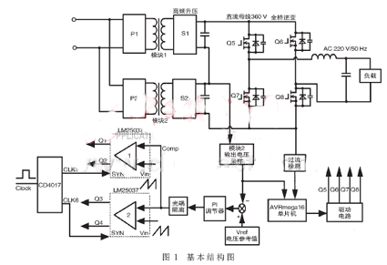
The system input is a 12 V DC battery with an output of 220 V/50 Hz. A typical secondary structure DC/DC high frequency boost and DC/AC low frequency inverter as shown in Figure 1 is employed. First, the DC/DC converter boosts the battery 12 V DC to 360 V; then the full-bridge SPWM inverter converts the DC power into an effective 220 V/50 Hz square wave for use by the load.
DC/DC circuit design
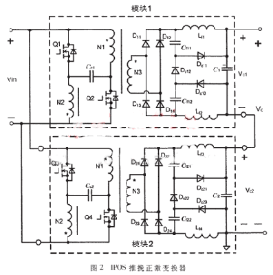
For high-voltage output applications, from the perspective of safety, a transformer isolated structure is generally used. The push-pull forward converter has the advantages of push-pull converter and forward converter. The transformer is bidirectionally excited and the core utilization is high. After adding the clamp capacitor, the voltage spike of the switch tube and the transformer bias problem can be effectively suppressed, and it is not necessary. The magnetic reset circuit has certain application value when inputting low voltage and high current [1, 2]. The input voltage of this system is 9.6~16 V DC, and the input current is about 50 A at full load. It is difficult to achieve high efficiency for a single push-pull forward converter. Therefore, the system uses a combined push-pull forward converter as shown in FIG. 2, that is, the input side parallel output side series IPOS. The IPOS structure has the following advantages: the primary side switch current stress is reduced; the two converters adopt an interleaved parallel control mode to reduce the input current ripple; the output side series structure reduces the output rectifier diode voltage stress [3]. The dual CDD absorbing circuit proposed in the reference [1] on the output side effectively suppresses the voltage spike caused by the reverse recovery of the rectifier diode, and facilitates selection of a diode with a lower rated voltage to reduce the conduction loss.
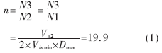
The DC/DC control circuit adopts the chip LM25037 designed by National Semiconductor for the vehicle power supply system. The chip has the following features: (1) wide range input operating voltage 5.5 V to 75 V; (2) before voltage can be used Feed mode or peak current mode control; (3) internal integrated feedforward PWM sawtooth generator; (4) programmable hysteresis undervoltage protection and dead time function; (5) timer dual mode with delay Overcurrent protection function; (6) Programmable maximum duty cycle and soft start; (7) Integrated high-precision error amplifier and overcurrent comparator with external synchronization; (8) 2-way alternate output The drive signal is suitable for topological structures such as push-pull, full-bridge and half-bridge [4].
The DC/DC converter is controlled by Common-duty ratio, and the output voltage of the control module 2 is stabilized at 180 V by the closed-loop regulation system. Using a decimal CD4017 divider to divide the 1 MHz input signal, two clock signals with a difference of 1/4T s are obtained as two external synchronization signals of the LM25037, and the output voltage error of the module 2 is adjusted by the PI as a two-chip control chip. The COMP terminal is given to realize the interleaving of two modules.
Transformer design
Design indicators: input voltage range 9.6 V ~ 16 V; output voltage Vo = 360 V; module 2 output voltage Vc2 = 180 V; power Po = 500 W; operating frequency fs = 50 kHz; maximum working duty Dmax = 0.47; The turns ratio of the transformer is:
The core of the ferrite ETD39 is actually selected, the turns ratio N=20, the primary side N1=N2=5åŒ, and the secondary side N3=100åŒ.
DC/DC output filter inductor design
According to the design requirements, the critical operating current Ioc=0.4, Io=0.28 A, and the output filter inductance value are:
![]()
The rear-stage full-bridge rectifier two-bridge arm is symmetrical, and the 1.4 mH inductor is divided into two identical 0.7 mH inductors wound on the same core. The ferrite EI30 core was selected, and the middle column was added with an air gap of 0.2 mm, and the number of turns was nf=65.
LM25037 peripheral circuit design
The peripheral circuit of the LM25037 is shown in Figure 3. The following is a detailed description of each part of the parameter selection.
Switching frequency and restart time setting
According to the chip data sheet, the switching frequency is f=50 kHz, the dead time is 250 ns, and the external clock frequency should be at least 10% higher than the free running frequency set by R6 in the external synchronous mode [4]. Select R6. =81 kΩ, R7=50 kΩ.
As shown in Figure 4, the restart time after overcurrent protection is determined by the following three parts:
(1) t1: When overcurrent, the internal 20 μA current source charges C9 to 2 V;
(2) t2: 1 μA current source charges C10 from 0 V to 1 V;
(3) t3: The current source of 100 μA charges C10 from 1 V to 5 V.
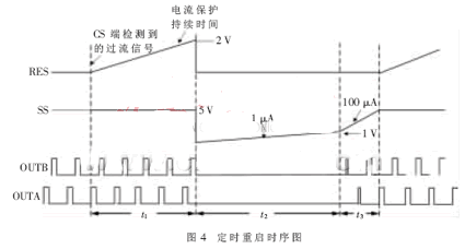
Therefore, by setting the values ​​of RES and SS pin capacitors C9 and C10, you can set the restart time after overcurrent protection. Taking C9=100 pF and C10=100 nF, the TRES is about 10.4 ms.
Feedforward network design
As shown in FIG. 5, the feedforward voltage signal charges C3 through an external RC network at each switching cycle input voltage to obtain a sawtooth wave whose slope is proportional to the input voltage. At the end of the switching cycle, C3 is discharged through the MOS transistor inside the chip to reset the capacitor.
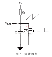
Take C3=100 pF, R3=200 kΩ, where Tdischarge<50 nS, Tsw is the oscillation period, VRAMP is the peak value of the ramp voltage, Vin is the input voltage, and Ron is the internal MOS tube on-resistance.
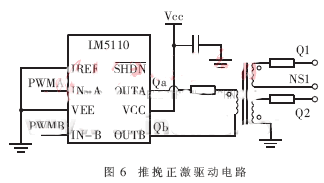
Drive circuit design
The push-pull forward converter drive is different from the push-pull circuit. For example, in the push-pull forward converter, when the grounded switch tube Q2 is turned on, the Q1 on the floating switch tube is subjected to -Vin, the general drive. The chip cannot withstand negative voltage, so the transformer is used to isolate the drive as shown in Figure 6. The leakage inductance should be considered in the design process of the drive transformer. The magnitude of the leakage inductance directly affects the speed of the drive signal, and the junction capacitance is oscillated when both switches are turned off, causing the switch tube to be mis-conducted. The maximum output current of the PWM output of the LM25037 is 50 mA. To prevent overheating of the chip in the isolated driver, a dedicated driver chip LM5110 is added. The drive circuit is shown in Figure 6.
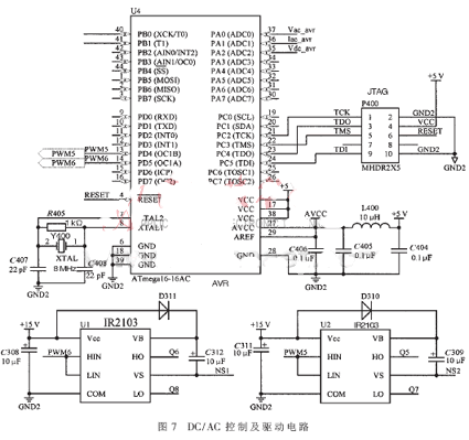
DC/AC circuit design
The inverter circuit is controlled by ATMEL's 8-bit AVRmega16 microcontroller. The device has two independent 8-bit timer/counters that can be pre-divided separately; one 16-bit timer/counter with comparison and capture; four PWM channels; and eight 10-bit ADCs.
The microcontroller control and inverter drive circuit are shown in Figure 7. In order to reduce the switching loss, the inverter adopts the unipolar frequency doubling modulation method, and uses the internal 16-bit timer T1 as two 8 bits, which can be obtained by comparing with two sine waves with a phase difference of 180°. A PWM signal that changes in a sinusoidal pattern. The reference sinusoidal signal is obtained by looking up the table. When the output voltage of the cigarette lighter is low, the DC bus voltage may not reach 360 V. Therefore, the feedforward control is used to judge different sine tables according to different bus voltage values ​​to ensure the output. The sine wave rms value is within the set range. T1a and T1b operate in phase-shifted PWM mode, and output pins OCR1A and OCR1B act as control signals for the inverter. In order to prevent the switch tube from passing through, a dead zone needs to be added between the upper and lower bridge arms of the switch tube. The drive chip IR2103 can easily realize the inversion of the signal, the 510 ns symmetric dead zone and the level conversion.
Experimental waveform
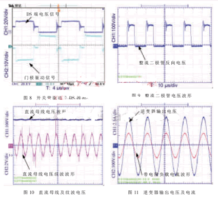
The following waveform is measured under the input voltage Vbat=12 VDC and the resistive load with output power Po=500 W at full load, and FIG. 8 is the voltage waveform of the forward converter switch and DS. It can be seen that due to the absorption of the clamp capacitor, the voltage spike of Vds is greatly reduced when the push-pull forward converter is turned off. Figure 9 shows the reverse voltage waveform that the rectifier diode is subjected to after the addition of the CDD snubber circuit. It can be seen that the clamp circuit effectively suppresses the reverse recovery of the diode, reducing voltage spikes and reverse recovery losses. Figure 10 shows the DC bus voltage and its ripple waveform at full load. The DC bus voltage ripple peak-to-peak value is about 4 V at full load. Figure 11 shows the voltage and current waveforms of the inverter output at full load. After analysis, the harmonic THD of the output voltage waveform is 0.97%, and the efficiency at full load is 85.7%.
The LM25037 portable vehicle inverter power supply proposed in this paper has the characteristics of high energy utilization, low THD, simple peripheral circuit and stable and reliable operation. It has certain application value in portable power supply.
As a mobile advertising display, Vehicle LED Display has precise advertising positioning and is widely used in public transport, taxis, case trains and family cars. It is widely used in outdoor image advertisement, information publication, activity advertisement, mobile background stage, information media and live broadcast of events, etc. its products are effective and flexible and widely used.

Features of Vehicle Led Display:
1. There is a unified operation background. Through GPS, you can know the specific location of each on-board screen. GPRS wireless replacement product content can play all the specified content partially. The above operations can be realized by computer and mobile phone
2. Mobile advertising has stronger communication and better effect. For vehicle mounted display screen, it has been in a state of motion, and advertising information has been more widely spread, with stronger communication ability and larger coverage area than fixed platform.
3. Vehicle Led Display adopts high brightness LED lamp beads, which can be seen clearly in the sun. The product has UV resistance in the sun, and the protection level reaches IP65, which is suitable for all-weather playback.
4. Ultra thin design of the product, allowing disassembly and assembly, reducing the space occupied in the car
5. Product module design, reliable and stable performance, power supply, system card, separate device, more stable product, more convenient maintenance
6. Led vehicle screen with GPS function can accurately know the screen position and operation status, including vehicle speed, driving direction, alarm status, etc.
7. Vehicle LED Display add brick and tile to the bright urban environment and become a beautiful scenic spot.

Original title of structure:
1. The screen adopts wide voltage, which can be applied to any vehicle in any occasion.
2. Single box design, according to customer requirements, can be iron box, can be aluminum box.
3. The system adopts group network function, which can control all vehicle screens individually. Even if the screen body is not in the same city, it can send specified and information through GPRS.
4. The screen body has an understanding of the lifting device, and the height can be adjusted according to the customer's requirements.

Vehicle LED Display
Led Display Panel,Vehicle Led Display,Led Screen Truck,Car Led Display
Shenzhen Vision Display Technology Co,.LTD , https://www.ledvdi.com