Existing system level EMI control technologies include:
1. Enclose the circuit in a Faraday box (note that the mechanical package containing the circuit should be sealed) to achieve EMI shielding;
2. Adopt filtering and attenuation techniques on the board or system I/O port to implement EMI control;
3. Strict shielding of the electric and magnetic fields of the circuit, or appropriate design techniques on the board to tightly control the capacitance and inductance of the PCB traces and board layers (self-shielding) to improve EMI performance.
EMI control usually requires a combination of the above techniques. In general, the closer to the EMI source, the lower the cost of implementing EMI control. The integrated circuit chip on the PCB is the primary source of energy for EMI, so EMI control in PCB and system-level designs can be simplified if the internal features of the integrated circuit chip are well understood.
PCB board and system level design engineers generally believe that the source of EMI they can access is the PCB. Obviously, at the PCB design level, a lot of work can be done to improve EMI. However, when considering EMI control, design engineers should first consider the choice of IC chips. Certain features of integrated circuits such as package type, bias voltage, and chip process technology (eg, CMOS, ECL, TTL) have a large impact on electromagnetic interference. This article will focus on these issues and explore the impact of ICs on EMI control.
Source of EMI
The frequency of the square wave signal generated at the output is not the only frequency component that causes EMI during the conversion of the digital integrated circuit from logic high to logic low or from logic low to logic high. The square wave contains a wide range of sinusoidal harmonic components, which constitute the EMI frequency component of interest to the engineer. The highest EMI frequency, also known as the EMI emission bandwidth, is a function of signal rise time rather than signal frequency. The formula for calculating the EMI emission bandwidth is:
F = 0.35 / Tr, where: F is the frequency, the unit is GHz; Tr is the signal rise time or fall time in ns (nanoseconds).
It is not difficult to see from the above formula that if the switching frequency of the circuit is 50 MHz and the rise time of the integrated circuit chip used is 1 ns, the highest EMI transmission frequency of the circuit will reach 350 MHz, which is much larger than the switching frequency of the circuit. And if the IC's rise time is 500ps, then the circuit's highest EMI emission frequency will be as high as 700MHz. It is well known that each voltage value in a circuit corresponds to a certain current, and each current has a corresponding voltage. When the output of the IC changes between logic high to logic low or logic low to logic high, these signal voltages and signal currents generate electric and magnetic fields, and the highest frequencies of these electric and magnetic fields are the emission bandwidth. The strength of the electric and magnetic fields and the percentage of external radiation are not only a function of the rise time of the signal, but also depend on the control of the capacitance and inductance of the signal path between the signal source and the load point. Here, the signal source is located on the PCB. Inside the board's IC, and the load is inside other ICs, these ICs may or may not be on the PCB. In order to effectively control EMI, it is necessary not only to pay attention to the capacitance and inductance of the IC chip itself, but also to pay attention to the capacitance and inductance existing on the PCB.
When the coupling between the signal voltage and the signal loop is not tight, the capacitance of the circuit is reduced, so that the suppression of the electric field is weakened, thereby increasing the EMI; the current in the circuit is also the same, if the current Poor coupling between the return path and the return path will inevitably increase the inductance on the loop, thereby enhancing the magnetic field and ultimately increasing EMI. In other words, poor control of the electric field often results in poor magnetic field suppression. The measures used to control the electromagnetic field in the board are similar to those used to suppress the electromagnetic field in the IC package. As with PCB design, IC package design will greatly affect EMI.
A significant portion of the electromagnetic radiation in the circuit is caused by voltage transients in the power bus. When the output stage of the IC hops and drives the connected PCB line to logic "high", the IC chip draws current from the power supply to provide the energy required by the output stage. For the ultra-high frequency current generated by the continuous conversion of the IC, the power bus starts from the decoupling network on the PCB and ends at the output stage of the IC. If the signal rise time of the output stage is 1.0 ns, then the IC must draw enough current from the power supply to drive the transmission line on the PCB in such a short period of 1.0 ns. The voltage transient on the power bus depends on the inductance on the power bus path, the current drawn, and the current transfer time. The voltage transient is defined by the following formula:
V = Ldi / dt, where: L is the value of the inductance on the current transmission path; di is the change in current during the signal rise time interval; dt is the transmission time of the current (rise time of the signal).
Since the IC pin and the internal circuit are both part of the power bus, and the rise time of the sinking current and the output signal is also determined to some extent depending on the process technology of the IC, the selection of a suitable IC can largely control the above formula. All three elements mentioned in the article.
The role of IC packaging in electromagnetic interference control
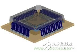
IC packages typically include: silicon-based chips, a small internal PCB, and pads. The silicon-based chip is mounted on a small PCB, and the connection between the silicon-based chip and the pad is realized by a bonding wire, and a direct connection can also be realized in some packages. The small PCB realizes the connection between the signal and power supply on the silicon-based chip and the corresponding pin on the IC package, thus realizing the external extension of the signal and power nodes on the silicon-based chip. The power and signal transmission paths throughout the IC include: silicon-based chips, wiring to small PCBs, PCB traces, and input and output pins for IC packages. The control of capacitance and inductance (corresponding to electric and magnetic fields) depends to a large extent on the design of the entire transmission path. Certain design features will directly affect the capacitance and inductance of the entire IC chip package.
First look at the connection between the silicon-based chip and the internal small circuit board. Many IC chips use a bonding wire to connect the silicon-based chip to the internal small circuit board, which is a very fine flying wire between the silicon-based chip and the internal small circuit board. This technique is widely used because the silicon-based chip and the internal small circuit board have similar thermal expansion coefficients (CTE). The chip itself is a silicon-based device with a coefficient of thermal expansion that is very different from the thermal expansion coefficient of a typical PCB material such as epoxy. If the electrical connection point of the silicon-based chip is directly mounted on the internal small PCB, then after a relatively short period of time, the internal temperature change of the IC package causes thermal expansion and contraction, and the connection in this way will fail due to the breakage. . Bound wire is a way of adapting to this special environment, it can withstand a lot of bending deformation and not easy to break.
The problem with bonded wires is that an increase in the current loop area of ​​each signal or power line will result in an increase in the inductance value. A good design for obtaining a lower inductance value is to achieve a direct connection between the silicon-based chip and the internal PCB, that is, the connection point of the silicon-based chip is directly bonded to the pad of the PCB. This requires the use of a special PCB board based material that should have a very low CTE. The choice of this material will lead to an increase in the overall cost of the IC chip, so chips using this process technology are not common, but as long as such an IC that directly connects the silicon-based chip to the carrier PCB exists and is feasible in the design, then The use of such an IC device is a better choice.
In general, in IC package design, reducing the inductance and increasing the capacitance between the signal and the corresponding loop or between the power supply and ground is the preferred consideration for selecting an integrated circuit chip process. For example, small-pitch surface mounts should be preferred over small-pitch surface mount packages when compared to large-pitch surface mount processes, which are packaged in two types of surface mount packages. IC chips are superior to over-hole lead type packages. The IC chip of the BGA package has the lowest lead inductance compared to any common package type. From the point of view of capacitance and inductance control, small packages and finer pitches often represent an increase in performance.
An important feature of lead structure design is the assignment of pins. Since the magnitude of the inductance and capacitance depends on the signal or the proximity between the power supply and the return path, consider enough return paths.
The power and ground pins should be allocated in pairs. Each power pin should have a corresponding ground pin adjacent to it, and multiple power and ground pin pairs should be assigned in this lead structure. Both of these features will greatly reduce the loop inductance between the power supply and ground, helping to reduce voltage transients on the power bus, thereby reducing EMI. Due to customary reasons, many IC chips on the market do not completely follow the above design rules. However, IC designers and manufacturers have a deep understanding of the advantages of this design method, so IC manufacturers are more likely to design and release new IC chips. Pay attention to the connection of the power supply.
Ideally, an adjacent signal return pin (such as a ground pin) should be assigned to each signal pin. This is not the case. Even the most avant-garde IC vendors do not allocate IC chips as such, but use other compromises. In the BGA package, a well-designed method is to set a signal return pin at the center of each set of eight signal pins. In this pin arrangement, between each signal and the signal return path. Only differ by one pin distance. For quad flat pack (QFP) or other gull wing type packages, it is unrealistic to place a signal return path in the center of the signal group, even if it is guaranteed every 4 to 6 Place a signal back to the pin. It should be noted that different IC process technologies may use different signal return voltages. Some ICs use ground pins (such as TTL devices) as the return path for signals, while some ICs use power pins (such as most ECL devices) as the return path for signals, and some ICs use both power and ground. Pins (such as most CMOS devices) act as a return path for the signal. Therefore, the design engineer must be familiar with the IC chip logic series used in the design to understand their related work.
The proper distribution of power and ground pins in the IC chip not only reduces EMI, but also greatly improves the ground bounce effect. When the device driving the transmission line attempts to pull the transmission line to a logic low, the ground bounce reflects the transmission line above the logic low threshold level, and the bounce reflection may cause the circuit to fail or malfunction.
Another important issue in IC packaging is the PCB design inside the chip. The internal PCB is usually the largest component of the IC package. If the internal PCB design can achieve strict control of capacitance and inductance, the design system will be greatly improved. Overall EMI performance. If this is a two-layer PCB board, at least one side of the PCB board is required to be a continuous ground plane layer, and the other layer of the PCB board is a wiring layer of power and signal. More ideally, a four-layer PCB board has two layers in the middle, a power supply and a ground plane, and two outer layers as signal wiring layers. Since the PCB inside the IC package is usually very thin, the design of the four-layer board structure will lead to two high-capacitance, low-inductance wiring layers, which are particularly suitable for power distribution and input and output signals that need to be strictly controlled to enter and exit the package. A low-impedance planar layer can greatly reduce voltage transients on the power bus, greatly improving EMI performance. This controlled signal line not only helps to reduce EMI, but also plays an important role in ensuring the integrity of the signal entering and leaving the IC.
Other related IC process technology issues
The integrated circuit chip bias and the driving power supply voltage Vcc are important issues to be aware of when selecting an IC. The current drawn from the IC power pin is mainly determined by the voltage value and the impedance of the transmission line (PCB line and ground return path) driven by the output stage of the IC chip. When the 5V power supply IC chip drives the 50Ω transmission line, the current drawn is 100mA; when the 3.3V power supply IC chip drives the same 50Ω transmission line, the absorption current will be reduced to 66mA; the 1.8V power supply IC chip drives the same 50Ω. When the line is transmitted, the sink current will be reduced to 36mA. It can be seen that in the formula V=Ldi/dt, the reduction of the drive current from 100 mA to 36 mA can effectively reduce the voltage transient V and thus reduce the EMI. Low-voltage differential signaling devices (LVDS) have signal voltage swings of only a few hundred millivolts, and it is conceivable that such device technology will have significant improvements in EMI.
The decoupling of power systems is also a problem that deserves special attention. The current drawn by the IC output stage through the power supply pins of the IC is provided by a decoupling network on the board. One possible way to reduce the voltage drop across the power bus is to shorten the distribution path between the decoupling capacitors and the IC output stage. This will reduce the "L" item in the "Ldi/dt" expression. Since the rise time of IC devices is getting faster, the only way to design PCBs is to minimize the distribution path between the decoupling capacitors and the IC output stage. One of the most straightforward solutions is to decouple all power supplies inside the IC. The ideal situation is to place it directly on the silicon-based chip and next to the driven output stage. For IC manufacturers, this is not only expensive but also difficult to implement. However, if the decoupling capacitor is placed directly on the PCB in the IC package and directly connected to the pins of the silicon-based chip, this design cost is minimized, contributing the most to EMI control and signal integrity. At present, only a few high-end microprocessors use this technology, but IC manufacturers are increasingly interested in this technology. It is foreseeable that such design technology will be widely used in future large-scale, high-power IC design.
Capacitors designed inside IC packages are usually small (less than a few hundred picofarads), so system designers still need to install decoupling capacitors between 0.001uF and 0.1uF on the PCB, but inside the IC package. Small capacitors suppress high-frequency components in the output waveform, which are the primary source of EMI.
Transmission line termination is also an important issue affecting EMI. Signal reflection can be reduced or eliminated by implementing terminal matching of the network line. Signal reflection is also an important factor affecting signal integrity. From the perspective of reducing EMI, the serial terminal matching effect is most obvious, because the terminal matching in this way reduces the incident wave (the original waveform propagating on the transmission line) to half of Vcc, thus reducing the need to drive the transmission line. Instantaneous absorption of current. This technique achieves the goal of reducing EMI by reducing the "di" term in "Ldi/dt".
Some IC manufacturers place termination matching resistors inside the IC package, which reduces the number of resistors on the PCB in addition to reducing EMI and improving signal integrity. Checking whether the IC chip uses such a technology can make the output impedance of the IC more clear. When the output impedance of the IC matches the impedance of the transmission line, it can be considered that such a transmission line implements "series termination matching". It is worth noting that the series-matched ICs use a reflection model of signal conversion. In practical applications, if there are multiple loads distributed along the transmission line direction and there are very strict timing requirements, then the serial terminal matching may not work.
Finally, the slope of the output signals of some IC chips is also controlled. For most TTL and CMOS devices, when their output stage signals are switched, the output transistors are fully turned on, which produces a large amount of transient current to drive the transmission line. Such a large surge current on the power bus is bound to produce very large voltage transients (V = Ldi / dt). Many ECL, MECL, and PECL devices drive the output stage by switching between the high and low levels of the linear region of the output transistor, commonly referred to as unsaturated logic. As a result, the peaks and valleys of the output waveform are flattened, thus reducing The amplitude of the high frequency harmonic component is reduced. This technique reduces EMI by increasing the signal rise time "dt" term in the expression "Ldi/dt".
to sum up
By carefully examining the package of the integrated circuit chip, the type of lead structure, the design method of the output driver, and the design method of the decoupling capacitor, useful design rules can be obtained. In the circuit design, attention should be paid to selecting and using electronic components that meet the following characteristics. :
· SMT or BGA package with very small form factor;
· The PCB inside the chip is a multi-layer PCB design with a power plane and a ground plane;
· The IC silicon-based chip is directly bonded to the internal small PCB (without bonding wires);
· Power and ground are paired side by side (to avoid power and ground appearing at the corners of the chip, such as the 74 series logic circuit);
· Multiple power and ground pins are configured in pairs;
· The signal return pin (such as the ground pin) is evenly distributed between the signal pins;
· Configure a dedicated signal return pin similar to a critical signal such as a clock;
· Use the lowest possible drive voltage (Vcc), such as 3.3V drive voltage or 5V differential logic (LVDS) for 5V;
· High frequency decoupling capacitors are used inside the IC package;
· Terminal matching of input and output signals on a silicon-based chip or inside an IC package;
· The slope of the output signal is controlled.
In summary, one of the most basic rules for selecting an IC device is to select the component with the longest rise time as long as it meets the timing requirements of the design system. Once the design engineer makes the final decision, but still can not determine the electromagnetic interference of the devices produced by different manufacturers of the same process technology, you can choose some devices from different manufacturers to do some testing. Install the IC chip in question on a specially designed test board to initiate clock operation and high-speed data manipulation. The electromagnetic emissions of the board can be easily tested by connecting to a near field magnetic loop probe on a spectrum analyzer or a wideband oscilloscope.
Plastic Capillary Pressure Gauge
Plastic Capillary Pressure Gauge,Mini-Sized Capillary Manometer,D28 Plastic Tube Pressure Gauge,Pipe Manometer
ZHOUSHAN JIAERLING METER CO.,LTD , https://www.zsjrlmeter.com