After decades of development, consumer electronics products have been used in countless types of equipment, from professional equipment to consumer goods. While there are differences in performance and functionality, consumer electronics tend to follow the same design trend: device capabilities are becoming more powerful, smaller, and less power efficient. The trend is exemplified by wearable devices, a portable, battery-powered, highly integrated device that takes everything from high-precision analog measurements to an intuitive user interface. Wearable device developers must carefully match the needs of their products across multiple integrated circuits (ICs), sometimes with conflicting preferences.
For example, let's think carefully about how size, battery life and functionality can be balanced in a smart wearable design without losing sight of the particularities of wearable devices: including their personalization and appeal. Let's take the example of a "single-function" type of wearable device - a pedometer with no screen or button battery power that alerts the user when they need to exercise, while still keeping track of the number of steps throughout the day. A simple capacitive sensing touch interface for user input, a three-color LED provides just enough expressive output, which allows the product to provide convenient and attractive personality features. This product design demonstrates how powerful ICs can be plugged into small packages to help promote innovation and product differentiation.
Our product requirements
Let us first outline the basic needs of the product. After defining the feature set, we are able to select the components responsible for each function. This is a pedometer that is streamlined to the basic functionality. There is no screen, buzzer or iPhone app available, the device deliberately highlights its simplicity and small size. Its user interface is also simple and straightforward.
Basic design requirements include:
• Minimize achievable form factor: Products with enclosures should be as close as possible to the CR2032 battery in all sizes, so users can carry the device in their pockets or hang on their keychain.
• User input: On the side of the button cell shape housing, provide a capacitive touch interface that recognizes the following inputs:
o Sliding: Unlock the alarm that the user needs to stand up
o Tap and hold: turn on a new day (reset pedometer)
o Tap: check the number of steps in a day
• Simple output: The exposed LEDs somewhere in the housing provide all the outputs:
o Red: A short flash of timing indicates that the user has been left still for too long.
o Green double flash: triggered by tapping and keeping the action when the user starts a new day
o 1 second red/yellow/green output: indicates the percentage of 33%, 66%, and 100% steps in a day, lasting a few seconds after tapping the touch interface
How to achieve miniaturization?
The CR2032 battery has a diameter of 20mm and a height of 3mm. Obviously, our system must be slightly larger than it, but how do we realize the miniaturization of wearable devices in reality? Let us assume that the plastic housing of the product can be made very thin, so it will not increase in length by more than 5mm in diameter, and it is easy to support battery replacement. For height, how do we minimize the height of the design and keep it as large as a button battery? In the vertical stacking of the product, its height consists of four device sizes: battery, printed circuit board (PCB), devices on the PCB, and the plastic housing of the product. For a four-layer PCB, the PCB thickness is approximately 0.5 mm. How to minimize the height of the device soldered to the PCB requires careful model selection. Finding devices in high-performance chip-scale packages is critical to our design.
Chip-level package benefits
The Wafer Level Chip Size Package (WLCSP) represents the result of years of continuous improvement in manufacturing and chip assembly technology. In the WLCSP package, silicon is directly connected to the solder balls on one side of the package. In contrast, the old technology connects the silicon port pads to the package pins through bond wires. The effect of this design is that the package can be designed to have a width and height that are close to the size of the internal silicon wafer itself.
IC vendors are scrambling to release the WLCSP's package to support a wide range of existing devices to achieve the benefits of a very small package type. The challenge that arises at this point is that some vendors' silicon chips are so large that they are not competitive in getting smaller packages. The EFM8SB1 MCU from Silicon Labs is well suited for the CSP package type because, although the MCU has a very high functional density, it has been adapted to small package sizes (eg 3mm & TImes; 3mm QFN package). The EFM8SB1 WLCSP package is only 1.78mm & TImes; 1.66mm.
The EFM8SB1 MCU is ideal for this and other wearable designs, and its key features include:
• 8-bit MCUs provide ultra-low power, high sensitivity capacitive sensing inputs.
• The on-chip real-time clock can periodically wake up the system from an ultra-low power (~300nA) state. In this design, one use of this clock is to measure the time since the last move and send an activity notification to encourage the user to stand up and move around.
• 2-8kB of flash and 512 bytes of RAM are maintained throughout the low power cycle. Combined with the 25MHz 8051 core, this small device has the ability to perform logic and perform multiple system responses.
Next is the choice of the pedometer. In order to make full use of the ultra-thin characteristics brought by the MCU of the CSP package, all the integrated circuits on the board must theoretically select the devices in the CSP package. For this reason, our onboard accelerometers should theoretically also support CSP packaging. The newly released Bosch BMA355 provides highly integrated sensors that enable a variety of three-axis event monitoring on-chip, with the ability to communicate with the EFM8 MCU via the SPI interface.
Because the two IC devices and the necessary discrete passive devices are available in an ultra-thin package, the plastic housing of the product can be made ultra-thin and close to the capacitive sensing surface to optimize touch sensitivity. The product's case even has a slight taper near the capacitive sensing pad area, creating a tiny gap between the PCB on the compression board and the on-board device.
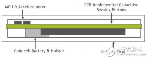
Figure 1: Vertical stack of wearable device boards with CSP MCUs
Board layout
Maximizing board space with CSP packaged devices allows us to implement capacitive sensing interfaces on the PCB. The MCU and accelerometer should be clustered on the edge of one side of the generally circular PCB, along with the bare LEDs. Of course, the LED may need to be opened in the package of the device to show.
In order to detect finger slippage, the board must have two capacitive sensors, theoretically two sensors of the same size, which are slightly staggered along their same edges. These two sensors should take up most of the area on the MCU side of the board, however they should be surrounded by a third small sensor, and this third sensor also surrounds the other two sensors. This third sensor provides the key information our MCU needs to perform during touch and slide detection during user interaction.
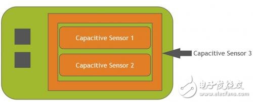
Figure 2: Wearable device board layout with capacitive sensor
Touch detection
The extreme portability of wearable devices means that these devices are usually placed on the body or in the hands. For devices that measure the proximity of a conductive material (such as a hand or skin), near-constant body contact detected by the device can cause touch detection problems. Fortunately, the features of the MCU and accelerometer chosen in the design help developers overcome these challenges.
Although the system has three capacitive sensors, it actually has four touch inputs. The accelerometer provides an interrupt-driven tap detector that can detect touch events via firmware and provide us with interfaces in a variety of ways. With the advantages of the accelerator tap detector, the touch detected by the EFM8SB1 MCU goes through the following stages:
• A positive increment is detected at the boundary sensor at the edge of the device, and an input use case is executed, where the user holds the device along the edge of the device or holds the palm of the device completely around the edge of the device, immediately following:
• Tap detection events are sent by the accelerometer and are consistent with the following events
• One or all of the capacitive sensors in the center detect a positive increase in significant amplitude
The MCU's firmware enables all capacitive sensing touch detection and filtering through the capacitive sensing firmware library provided by the Silicon Labs Simplicity Studio development environment.
Low power function
Both the accelerometer and the MCU can be configured to operate in low power mode. The Capacitive Sensing Firmware Library enables the EFM8SB1 MCU to enter a ~300nA sleep mode and periodically wake up to check for activity events on the capacitive sensor. If the accelerometer signals that the event has been detected and the data is ready, the MCU can also use the port match wake event to asynchronously wake up.
The EFM8SB1 MCU will remain in a low power state and consume less than 1μA of current unless one of the following conditions occurs:
• Touch detection events require more response to capacitive sensing input monitoring
• Accelerometer activity events (such as tap detection or footstep detection interrupts) require MCU wake-up to service these interrupts
• Motion notification events, device switch LEDs to encourage users to stand up and move around
At the same time, the accelerometer is configured to implement the lowest power consumption operating state while transmitting the signal only during a tap event or when one of the three axes detects a change. But on-chip cache data minimizes the number of interactions between the MCU and the accelerometer, further optimizing battery life.
After the MCU reads the buffered data from the accelerometer, some additional checks and analyses must be performed to determine if there are subsequent steps. Once the three-axis data is compared to the historical data stored on the EFM8SB1 device, the MCU can update its pedometer and quickly return to the low power state.
Next step?
This example shows a "single-function" type of end product in the field of wearable devices. The functional density, accuracy, and energy efficiency of CSP-sized integrated circuit operation in the examples also illustrates how to use and control such ICs. For example, a product described in a wearable design can be considered as a subsystem in a larger product where a chip-sized MCU can operate as a low-power sensor hub to manage touch interfaces and accelerometers. As silicon chip vendors try to integrate more features into smaller packages, system developers need to take advantage of these innovations to get inspiration for product design.
Various products of Crystal Usb Flash Drive, including Crystal USB Flash Drive Gift Box, Crystal Usb Logo, Crystal Usb Stick, Crystal Usb Memory Stick, Crystal Usb 2.0 Memory Flash Stick Pen Drive and so on. We also providing product images and basic parameters with each Crystal USB Flash Drive and Crystal USB Flash Drive OEM 3D inside engraved Logo;

Crystal USB Flash Drive is An ideal way to store all your pictures, documents, music and videos. Crystal USB Flash Drive Can act as a wonderful gift for your friends and families and A great way to distinguish your masses of USB flash drives from each other as our cute USB come in a variety of variations for every day use.

- Compatibility: Desktop, Laptop, Macintosh, Tablet, Speakers all with USB1.0 and 2.0.
- Operating System : Windows7/Vista/XP/2000/ME/NT/98,Linux (Sometimes incompatible with Mac OS 9.X/Linux2.4)
- Fine choice for advertisement allow to print LOGOs and advertisement.
- Very Low Power Consumption, durable solid-state storage.
- Small and exquisite design brings much convenience.
We are a professional Chinese manufacturer of Crystal USB Flash Drive, and look forward to your cooperation!

Crystal Usb Flash Drive
Crystal Usb Flash Drive, Bulb Shape Crystal Usb Flash Drive,3D Laser Crystal Usb Flash Drive
Reteck Electronic Co., Ltd. , https://www.reteck.com