ADSP21160 realizes digital signal processing system
This paper uses ADI's ADSP21160 as the main processor to build a signal processing hardware platform, and gives the system concept and specific circuit design, which has certain practical value.
The ADSP21160 adopts a super Harvard architecture. There are 4 independent buses on the chip for dual data access, instruction access and input/output interfaces. The processor core is integrated on the chip (including arithmetic unit, control unit and address generator). Main blocks of digital information processing systems such as buses, interrupts, registers, etc., large-capacity dual-port static memories, program/data external buses and multiprocessor interfaces, and input/output controllers.
Hardware system design ideas
The following is a brief introduction to the design of the system from the data input and output, system power-on operation, system power configuration and circuit control.
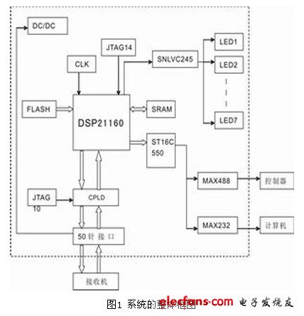
1. Consider the data transfer first. The external device (receiver) processes the data through the ADSP21160 through a 50-pin interface and converts it into a serial data output for transmission to peripherals (controllers) and computers. For the confidentiality of the circuit system and the implementation of some logic control circuits in the system, a CPLD control circuit is added between the ADSP21160 and the 50-pin interface.
2. In order to run the system itself after power-on, you need to configure an external FLASH for the DSP, and pre-program the calculation program in FLASH. By configuring the ADSP21160 boot mode, after the system is powered on, the ADSP21160 can automatically read and run the program from FLASH.
3. Since the ADSP21160 has only 4Mbit of internal storage space, it is divided into two parts: data storage space and program storage space. In order to facilitate the future upgrade of the system and program, SRAM is configured with 512K & TImes; 32-bit external storage space.
4. Since the serial port of the ADSP21160 is not a general-purpose UART serial port, and both the system and the computer require serial data output, a parallel-serial conversion chip is required in the system to output the operation result.
5. Since the external only provides +5V DC power supply, and the ADSP21160 requires +3.3V interface power supply and 2.5V core power supply, the system internal device also chooses +3.3V device as much as possible, so the system needs a DC/DC conversion chip. Convert +5V power to +2.5V and +3.3V power output.
System function module design
1. Power module design
In the system design, since the external interface power supply of the ADSP21160 is +3.3V, in order to simplify the circuit and improve the performance of the circuit board, the +3.3V device is also selected as much as possible in the selection of other devices. A few devices that are difficult to find a +3.3V power supply have chosen a +5V device without affecting the interface and functionality. In addition, the ADSP21160 requires a +2.5V core power supply and a +2.5V analog power supply (for the ADSP21160's internal phase-locked loop). The external power supply is +5V. Considering the above requirements, the system needs a DC/DC converter module that outputs +3.3V and +2.5V voltage, and divides the +2.5V power supply into digital and analog two channels.
The ADSP21160 requires the core power supply to be powered earlier than the external port, otherwise the DSP may be booting abnormally or the program may not load. Therefore, considering this problem in the power supply design, it is decided to use the +2.5V output terminal of DC/DC to connect to the +3.3V output enable terminal through the delay circuit, which solves this problem well.
Based on the specific requirements of the integrated system for voltage and current, the hardware system selected TI's TPS767D301 as the DC/DC converter chip. Its input is +5V voltage, output one +3.3V voltage and one channel +1.8V or +2.5V adjustable voltage, the maximum current output is 1A.
2.DSP main module design
Clock Drive: The ADSP21160 requires an external clock driver, so an external clock is essential. Its internal phase-locked loop setting multiplies the internal operating frequency to 2, 3 or 4 times the external clock frequency. The highest core clock frequency is 80MHz. In this way, the high-speed operation of the core processor can be realized with a low external frequency (data transmission frequency).
In this system, in order to improve the high-frequency interference capability of the system and reduce the design difficulty of the system, it has little effect on the system running speed (since the main time-consuming of the system is concentrated on the processing of the matrix, the data transmission is relatively In terms of only one-tenth of its total operating time, the externally selects a 20MHz drive clock, and then sets the internal phase-locked loop to four times the external clock to achieve high-speed internal operations.
Program loading: ADSP21160 needs an external 14-pin JTAG interface. By using the ICE simulator provided by Analog Devices, the compiled user program is downloaded from the computer and loaded into the internal memory of the ADSP21160 or external FLASH.
External Device Gating: The ADSP21160 is configured with four external pins, /MS3~/MS0, for gating of external devices. At the same time, only one of them is allowed to be active (low level). These pins are connected to the enable terminals of the FLASH, SRAM, and parallel-to-serial conversion chips (ST16C550) for gating these components and for data communication with external receivers. Because of the logic function of several devices, CPLD is in a working state for a long time (the enable terminal is directly grounded).
3.FLASH loading and expansion memory module design
FLASH load module: In order to automatically run the system after power-on, the external DSP is configured for the ADSP21160. According to the ADSP21160 user manual, the 8-bit FLASH data line is connected to the 32_39 bit of the DSP data line. The address line must be directly connected to the ADSP21160 corresponding address bit from ADDR0. The ADSP21160 uses the EPROM boot mode, with /BMS and /MS0 phase and back connected to the FLASH enable.
External Memory Module: The ADSP21160 is a high-performance 32-bit floating-point processor that can use up to 64-bit data bus. Taking into account the accuracy requirements of the system and the processing mode of internal data, the system only uses a 32-bit data bus. Thus, in the selection of the external expansion memory, considering the price and other factors, two 256K & TImes are selected; the 16-bit SRAM is connected in parallel to form a 32-bit external expansion memory, as shown in FIG. 2 .
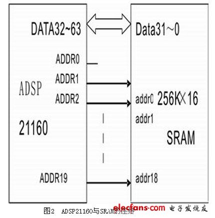
On the connection of the address line, it is different from the general connection. Since the ADSP21160 specifies that the external space is addressed, its odd address is passed through the lower 32-bit data line; the even address is passed through the upper 32-bit data line. Considering that the 32_39 bit of the DSP data line is used in the FLASH connection, in order to simplify the wiring of the PCB in the future and make full use of the storage space of the SRAM, in the design, the ADDR0 pin of the ADSP21160 is suspended, and its ADDR1 pin is The addr0 pin of the SRAM is connected, and the ADDR2 is connected to the addr1, and the following are sequentially connected.
We are 1050nm LED manufacturer from China.
We will do the High temperature resistance testing and 10
hours ageing treatment before the product out off the factory, which can
ensure the stability of each product.
Our LED products have 5 year warranty.
We are the best supplier for your light-emitting diode.
For the Through-hole Light Emitting Diode 1050nm LED,
We can customize the shape, the lighting angle, the number of emitting source, the flat pin LED and braided LED. Such as: infrared 5mm 1050nm LED with 5 degree, infrared 5mm 1050nm LED with 20 degree, infrared 5mm 1050nm LED with 30 degree, infrared 5mm 1050nm LED with 45 degree, infrared 5mm 1050nm LED with 60 degree, infrared 5mm 1050nm with 90 degree, infrared 5mm 1050nm LED with 120 degree. Infrared 3mm 1050nm LED with 3 degree, infrared 3mm 1050nm LED with 20 degree, infrared 3mm 1050nm LED with 30 degree, infrared 3mm 1050nm LED with 45 degree, infrared 3mm 1050nm LED with 60 degree, infrared 3mm 1050nm with 90 degree, infrared 3mm 1050nm LED with 120 degree ect.
There are many other shapes or color of lens for your choose. Customized infrared LED are available
For the SMD LED 1050nm LED,
We can supply dual-chip infrared LED, three-chip infrared LED, multi-chip infrared LED, high voltage LED, flashing infrared LED and variety of size SMD LED. For instance: 3528 SMD infrared 1050nm LED, 2835 SMD infrared 1050nm LED, 3014 SMD infrared 1050nm LED, 1206 SMD infrared 1050nm LED, 3020 SMD infrared 1050nm LED.
There are also have many other shapes to choose, like the 5050 SMD infrared LED, the 5730 SMD infrared LED ect. You can choose any one of them for your requirement.
1050nm led is a infrared LED( IR LED ). Common infrared LEDs are like: 1050nm IR LED, 1100nm IR LED and so on.
1050nm LED
1050nm IR LED, 1050nm LED, 1050nm Infrared LED, 3W 1050nm LED, 1050nm Light Emitting Diode
Shenzhen Best LED Opto-electronic Co.,Ltd , https://www.bestsmd.com